参数资料
| 型号: | MAX1401EAI+T |
| 厂商: | Maxim Integrated Products |
| 文件页数: | 34/36页 |
| 文件大小: | 0K |
| 描述: | IC ADC 18BIT LP 28-SSOP |
| 产品培训模块: | Lead (SnPb) Finish for COTS Obsolescence Mitigation Program |
| 标准包装: | 2,000 |
| 位数: | 18 |
| 采样率(每秒): | 480 |
| 数据接口: | QSPI?,串行,SPI? |
| 转换器数目: | 1 |
| 功率耗散(最大): | 750µW |
| 电压电源: | 模拟和数字 |
| 工作温度: | -40°C ~ 85°C |
| 安装类型: | 表面贴装 |
| 封装/外壳: | 28-SSOP(0.209",5.30mm 宽) |
| 供应商设备封装: | 28-SSOP |
| 包装: | 带卷 (TR) |
| 输入数目和类型: | 3 个差分,单极;3 个差分,双极;5 个伪差分,单极;5 个伪差分,双极 |
第1页第2页第3页第4页第5页第6页第7页第8页第9页第10页第11页第12页第13页第14页第15页第16页第17页第18页第19页第20页第21页第22页第23页第24页第25页第26页第27页第28页第29页第30页第31页第32页第33页当前第34页第35页第36页
ns
MAX1401
+3V, 18-Bit, Low-Power, Multichannel,
Oversampling (Sigma-Delta) ADC
_______________________________________________________________________________________
7
Note 16: These specifications apply to CLKOUT only when driving a single CMOS load.
Note 17: The burn-out currents require a 500mV overhead between the analog input voltage and both V+ and AGND to operate
correctly.
Note 18: Measured at DC in the selected passband. PSR at 50Hz will exceed 120dB with filter notches of 25Hz or 50Hz and FAST
bit = 0. PSR at 60Hz will exceed 120dB with filter notches of 20Hz or 60Hz and FAST bit = 0.
Note 19: PSR depends on gain. For a gain of +1V/V, PSR is 70dB typical. For a gain of +2V/V, PSR is 75dB typical. For a gain of
+4V/V, PSR is 80dB typical. For gains of +8V/V to +128V/V, PSR is 85dB typical.
Note 20: Standby power-dissipation and current specifications are valid only with CLKIN driven by an external clock and with the
external clock stopped. If the clock continues to run in standby mode, the power dissipation will be considerably higher.
When used with a resonator or crystal between CLKIN and CLKOUT, the actual power dissipation and IDD in standby
mode will depend on the resonator or crystal type.
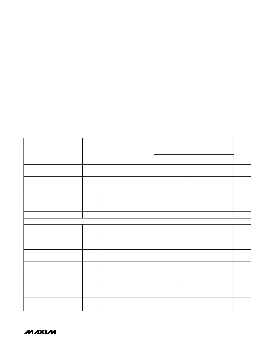
TIMING CHARACTERISTICS
(V+ = +2.7V to +3.6V, VDD = +2.7V to +3.6V, AGND = DGND, fCLKIN = 2.4576MHz, input logic 0 = 0V, logic 1 = VDD, TA = TMIN to
TMAX, unless otherwise noted.) (Notes 21, 22, 23)
0100
Bus-Relinquish Time After SCLK
Rising Edge (Note 28)
t10
10
100
ns
SCLK Falling Edge to Data Valid
Delay (Notes 26, 27)
t6
ns
INT High Time
tINT
560 / N
tCLKIN
ns
X2CLK = 1, N = 2(2 MF1 + MF0)
X2CLK = 1
X2CLK = 0
SCLK Setup to Falling Edge CS
t4
30
ns
SCLK Low Pulse Width
t8
100
ns
CS Rising Edge to SCLK Rising
Edge Hold Time (Note 23)
t9
0
ns
SCLK High Pulse Width
t7
100
ns
CS Falling Edge to SCLK Falling
Edge Setup Time
t5
30
ns
280 / N
tCLKIN
INT to CS Setup Time (Note 10)
t3
X2CLK = 0, N = 2(2 MF1 + MF0)
0
ns
RESET Pulse Width Low
t2
100
ns
Master Clock Input Low Time
fCLKIN LO
0.4
tCLKIN
ns
tCLKIN = 1 / fCLKIN, X2CLK = 0
Master Clock Input High Time
fCLKIN HI
0.4
tCLKIN
ns
tCLKIN = 1 / fCLKIN, X2CLK = 0
Master Clock Frequency
fCLKIN
0.8
5.0
MHz
Crystal oscillator or clock
externally supplied for
specified performance
(Notes 24, 25)
PARAMETER
SYMBOL
MIN
TYP
MAX
UNITS
0.4
2.5
CONDITIONS
SCLK Rising Edge to INT High
(Note 29)
t11
200
ns
SERIAL-INTERFACE READ OPERATION
相关PDF资料 |
PDF描述 |
|---|---|
| V24B5M150BG | CONVERTER MOD DC/DC 5V 150W |
| MS3102R36-15S | CONN RCPT 35POS BOX MNT W/SCKT |
| MAX1189CCUI+ | IC ADC 16BIT 135KSPS 28-TSSOP |
| MS3102E36-15S | CONN RCPT 35POS BOX MNT W/SCKT |
| MS27505E11F13P | CONN RCPT 13POS BOX MNT W/PINS |
相关代理商/技术参数 |
参数描述 |
|---|---|
| MAX1402CAI | 功能描述:ADC / DAC多通道 RoHS:否 制造商:Texas Instruments 转换速率: 分辨率:8 bit 接口类型:SPI 电压参考: 电源电压-最大:3.6 V 电源电压-最小:2 V 最大工作温度:+ 85 C 安装风格:SMD/SMT 封装 / 箱体:VQFN-40 |
| MAX1402CAI+ | 功能描述:模数转换器 - ADC 18-Bit 5Ch 4.8ksps 2.5V Precision ADC RoHS:否 制造商:Texas Instruments 通道数量:2 结构:Sigma-Delta 转换速率:125 SPs to 8 KSPs 分辨率:24 bit 输入类型:Differential 信噪比:107 dB 接口类型:SPI 工作电源电压:1.7 V to 3.6 V, 2.7 V to 5.25 V 最大工作温度:+ 85 C 安装风格:SMD/SMT 封装 / 箱体:VQFN-32 |
| MAX1402CAI+T | 功能描述:模数转换器 - ADC 18-Bit 5Ch 4.8ksps 2.5V Precision ADC RoHS:否 制造商:Texas Instruments 通道数量:2 结构:Sigma-Delta 转换速率:125 SPs to 8 KSPs 分辨率:24 bit 输入类型:Differential 信噪比:107 dB 接口类型:SPI 工作电源电压:1.7 V to 3.6 V, 2.7 V to 5.25 V 最大工作温度:+ 85 C 安装风格:SMD/SMT 封装 / 箱体:VQFN-32 |
| MAX1402CAI-T | 功能描述:ADC / DAC多通道 RoHS:否 制造商:Texas Instruments 转换速率: 分辨率:8 bit 接口类型:SPI 电压参考: 电源电压-最大:3.6 V 电源电压-最小:2 V 最大工作温度:+ 85 C 安装风格:SMD/SMT 封装 / 箱体:VQFN-40 |
| MAX1402EAI | 功能描述:ADC / DAC多通道 RoHS:否 制造商:Texas Instruments 转换速率: 分辨率:8 bit 接口类型:SPI 电压参考: 电源电压-最大:3.6 V 电源电压-最小:2 V 最大工作温度:+ 85 C 安装风格:SMD/SMT 封装 / 箱体:VQFN-40 |
发布紧急采购,3分钟左右您将得到回复。