参数资料
| 型号: | MAX1401EAI+T |
| 厂商: | Maxim Integrated Products |
| 文件页数: | 33/36页 |
| 文件大小: | 0K |
| 描述: | IC ADC 18BIT LP 28-SSOP |
| 产品培训模块: | Lead (SnPb) Finish for COTS Obsolescence Mitigation Program |
| 标准包装: | 2,000 |
| 位数: | 18 |
| 采样率(每秒): | 480 |
| 数据接口: | QSPI?,串行,SPI? |
| 转换器数目: | 1 |
| 功率耗散(最大): | 750µW |
| 电压电源: | 模拟和数字 |
| 工作温度: | -40°C ~ 85°C |
| 安装类型: | 表面贴装 |
| 封装/外壳: | 28-SSOP(0.209",5.30mm 宽) |
| 供应商设备封装: | 28-SSOP |
| 包装: | 带卷 (TR) |
| 输入数目和类型: | 3 个差分,单极;3 个差分,双极;5 个伪差分,单极;5 个伪差分,双极 |
第1页第2页第3页第4页第5页第6页第7页第8页第9页第10页第11页第12页第13页第14页第15页第16页第17页第18页第19页第20页第21页第22页第23页第24页第25页第26页第27页第28页第29页第30页第31页第32页当前第33页第34页第35页第36页
MAX1401
+3V, 18-Bit, Low-Power, Multichannel,
Oversampling (Sigma-Delta) ADC
6
_______________________________________________________________________________________
Note 1:
Contact factory for INL limits applicable with FS1 = 0 and MF1, MF0 = 1, 2, or 3.
Note 2:
To achieve optimum INL performance with the MAX1401, ensure that the PCB layout carefully shields the MUXOUT and
ADCIN pins from any digital noise source. The MAX1401’s INL is production tested with 150pF connected between
MUXOUT+ and MUXOUT- to minimize the effect of differential coupling from the CLKIN and CLKOUT pins.
Note 3:
Nominal gain is 0.98. This ensures a full-scale input voltage may be applied to the part under all conditions without caus-
ing saturation of the digital output data.
Note 4:
Positive Full-Scale Error includes zero-scale errors (unipolar offset error or bipolar zero error) and applies to both unipolar
and bipolar input ranges. This error does not include the nominal gain of 0.98.
Note 5:
Full-Scale Drift includes zero-scale drift (unipolar offset drift or bipolar zero drift) and applies to both unipolar and bipolar
input ranges.
Note 6:
Gain Error does not include zero-scale errors. It is calculated as (full-scale error - unipolar offset error) for unipolar ranges
and as (full-scale error - bipolar zero error) for bipolar ranges. This error does not include the nominal gain of 0.98.
Note 7:
Gain-Error Drift does not include unipolar offset drift or bipolar zero drift. It is effectively the drift of the part if zero-scale
error is removed.
Note 8:
Use of the offset DAC does not imply that any input may be taken below AGND.
Note 9:
Additional noise added by the offset DAC is dependent on the filter cutoff, gain, and DAC setting. No noise is added for a
DAC code of 0000.
Note 10: Guaranteed by design or characterization; not production tested.
Note 11: The input voltage must be within the Absolute Input Voltage Range specification.
Note 12: All AIN and REFIN pins have identical input structures. Leakage is production tested only for the AIN3, AIN4, AIN5,
CALGAIN, and CALOFF inputs.
Note 13: The dynamic load presented by the MAX1401 analog inputs for each gain setting is discussed in detail in the Switching
Network section. Values are provided for the maximum allowable external series resistance. Note that this value does not
include any additional capacitance added by the user to the MUXOUT_ or ADCIN_ pins.
Note 14: The input voltage range for the analog inputs is with respect to the voltage on the negative input of its respective differen-
tial or pseudo-differential pair. Table 5 shows which inputs form differential pairs.
Note 15: VREF = VREFIN+ - VREFIN-.
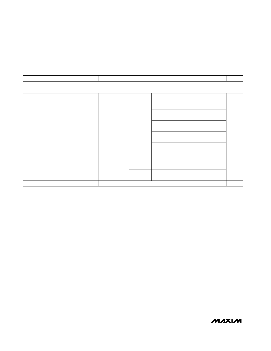
ELECTRICAL CHARACTERISTICS (continued)
(V+ = +2.7V to +3.6V, VDD = +2.7V to +3.6V, VREFIN+ = +1.25V, REFIN- = AGND, fCLKIN = 2.4576MHz, TA = TMIN to TMAX, unless
otherwise noted. Typical values are at TA = +25°C.)
2.4576MHz
1.024MHz
Buffers off
Buffers on
2.4576MHz
1.024MHz
1.45
2.05
Buffers off
Buffers on
Normal mode,
MF1 = 0,
MF0 = 0
2.51
3.30
1.32
1.98
Buffers on
2.28
Buffers on
2X mode,
MF1 = 0,
MF0 = 1
4.53
6.11
CONDITIONS
1.95
2.97
1.08
2.4576MHz
1.024MHz
Buffers off
Buffers on
2.4576MHz
1.024MHz
4.32
Buffers off
Buffers on
4X mode,
MF1 = 1,
MF0 = 0
16.6
21.2
6.67
8.58
Buffers on
16.4
Buffers on
8X mode,
MF1 = 1,
MF0 = 1
mW
16.9
21.45
PD
Power Dissipation
7.0
8.91
6.44
1.75
(Note 20)
770
W
Standby Power Dissipation
0.81
1.36
UNITS
MIN
TYP
MAX
SYMBOL
PARAMETER
POWER DISSIPATION (V+ = VDD = +3.3V, digital inputs = 0 or VDD, external CLKIN, burn-out currents disabled, X2CLK = 0,
CLK = 0 for 1.024MHz, CLK = 1 for 2.4576MHz.)
相关PDF资料 |
PDF描述 |
|---|---|
| V24B5M150BG | CONVERTER MOD DC/DC 5V 150W |
| MS3102R36-15S | CONN RCPT 35POS BOX MNT W/SCKT |
| MAX1189CCUI+ | IC ADC 16BIT 135KSPS 28-TSSOP |
| MS3102E36-15S | CONN RCPT 35POS BOX MNT W/SCKT |
| MS27505E11F13P | CONN RCPT 13POS BOX MNT W/PINS |
相关代理商/技术参数 |
参数描述 |
|---|---|
| MAX1402CAI | 功能描述:ADC / DAC多通道 RoHS:否 制造商:Texas Instruments 转换速率: 分辨率:8 bit 接口类型:SPI 电压参考: 电源电压-最大:3.6 V 电源电压-最小:2 V 最大工作温度:+ 85 C 安装风格:SMD/SMT 封装 / 箱体:VQFN-40 |
| MAX1402CAI+ | 功能描述:模数转换器 - ADC 18-Bit 5Ch 4.8ksps 2.5V Precision ADC RoHS:否 制造商:Texas Instruments 通道数量:2 结构:Sigma-Delta 转换速率:125 SPs to 8 KSPs 分辨率:24 bit 输入类型:Differential 信噪比:107 dB 接口类型:SPI 工作电源电压:1.7 V to 3.6 V, 2.7 V to 5.25 V 最大工作温度:+ 85 C 安装风格:SMD/SMT 封装 / 箱体:VQFN-32 |
| MAX1402CAI+T | 功能描述:模数转换器 - ADC 18-Bit 5Ch 4.8ksps 2.5V Precision ADC RoHS:否 制造商:Texas Instruments 通道数量:2 结构:Sigma-Delta 转换速率:125 SPs to 8 KSPs 分辨率:24 bit 输入类型:Differential 信噪比:107 dB 接口类型:SPI 工作电源电压:1.7 V to 3.6 V, 2.7 V to 5.25 V 最大工作温度:+ 85 C 安装风格:SMD/SMT 封装 / 箱体:VQFN-32 |
| MAX1402CAI-T | 功能描述:ADC / DAC多通道 RoHS:否 制造商:Texas Instruments 转换速率: 分辨率:8 bit 接口类型:SPI 电压参考: 电源电压-最大:3.6 V 电源电压-最小:2 V 最大工作温度:+ 85 C 安装风格:SMD/SMT 封装 / 箱体:VQFN-40 |
| MAX1402EAI | 功能描述:ADC / DAC多通道 RoHS:否 制造商:Texas Instruments 转换速率: 分辨率:8 bit 接口类型:SPI 电压参考: 电源电压-最大:3.6 V 电源电压-最小:2 V 最大工作温度:+ 85 C 安装风格:SMD/SMT 封装 / 箱体:VQFN-40 |
发布紧急采购,3分钟左右您将得到回复。