- 您现在的位置:买卖IC网 > PDF目录15488 > MAX1858EEG+ (Maxim Integrated Products)IC REG CTRLR BUCK PWM VM 24-QSOP PDF资料下载
参数资料
| 型号: | MAX1858EEG+ |
| 厂商: | Maxim Integrated Products |
| 文件页数: | 17/21页 |
| 文件大小: | 0K |
| 描述: | IC REG CTRLR BUCK PWM VM 24-QSOP |
| 产品培训模块: | Lead (SnPb) Finish for COTS Obsolescence Mitigation Program |
| 标准包装: | 50 |
| PWM 型: | 电压模式 |
| 输出数: | 2 |
| 频率 - 最大: | 660kHz |
| 占空比: | 90% |
| 电源电压: | 4.75 V ~ 23 V |
| 降压: | 是 |
| 升压: | 无 |
| 回扫: | 无 |
| 反相: | 无 |
| 倍增器: | 无 |
| 除法器: | 无 |
| Cuk: | 无 |
| 隔离: | 无 |
| 工作温度: | -40°C ~ 85°C |
| 封装/外壳: | 24-SSOP(0.154",3.90mm 宽) |
| 包装: | 管件 |
�� �
�
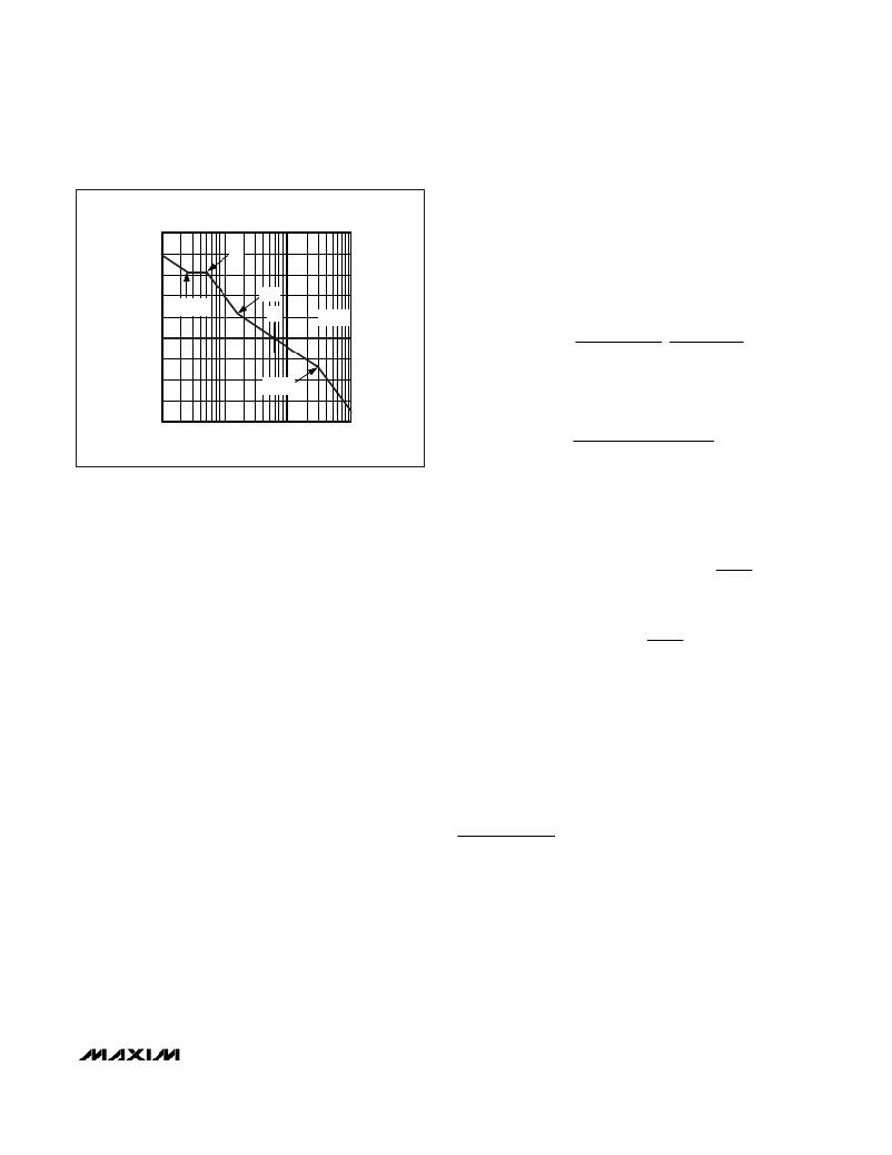
�Dual� 180°� Out-of-Phase� PWM� Step-Down�
�Controller� with� Power� Sequencing� and� POR�
�50�
�40�
�30�
�BODE� PLOT� FOR� VOLTAGE-�
�MODE� CONTROLLERS�
�f� LC�
�Calculate� MOSFET� temperature� rise� according� to� pack-�
�age� thermal-resistance� specifications� to� ensure� that�
�both� MOSFETs� are� within� their� maximum� junction� tem-�
�perature� at� high� ambient� temperature.� The� worst-case�
�dissipation� for� the� high-side� MOSFET� (P� NH� )� occurs� at�
�both� extremes� of� input� voltage,� and� the� worst-case� dis-�
�P� NH� (� SWITCHING� )� =� IN� LOAD� OSC� ?� GS� GD� ?�
�20�
�10�
�0�
�-10�
�-20�
�-30�
�f� Z-COMP_A�
�f� ESR�
�f� CO�
�f� COMP_B�
�f� SWITCH�
�sipation� for� the� low-side� MOSFET� (P� NL� )� occurs� at� maxi-�
�mum� input� voltage.�
�V� I� f� ?� Q� +� Q� ?�
�2� ?� I� GATE� ?�
�I� GATE� is� the� average� DH� driver� output� current� capability�
�determined� by:�
�(�
�-40�
�0.001�
�0.01� 0.1�
�FREQUENCY� (MHz)�
�1�
�I� GATE� =�
�V� L�
�2� R� DS� (� ON� )� DH� +� R� GATE�
�)�
�P� NH� (� CONDUCTION� )� =� I� LOAD� 2� R� DS� (� ON� )� NH� ?� OUT� ?�
�P� NL� =� I� LOAD� 2� R� DS� (� ON� )� NL� ?� 1-� ?� OUT� ?� ?�
�Figure 8. Voltage-Mode Loop Analysis�
�All� four� N-channel� MOSFETs� must� be� a� logic-level� type�
�with� guaranteed� on-resistance� specifications� at� V� GS� ≥�
�4.5V.� For� maximum� efficiency,� choose� a� high-side�
�MOSFET� (N� H� _)� that� has� conduction� losses� equal� to� the�
�switching� losses� at� the� optimum� input� voltage.� Check� to�
�ensure� that� the� conduction� losses� at� minimum� input�
�voltage� do� not� exceed� MOSFET� package� thermal� limits,�
�or� violate� the� overall� thermal� budget.� Also,� check� to�
�ensure� that� the� conduction� losses� plus� switching� losses�
�at� the� maximum� input� voltage� do� not� exceed� package�
�ratings� or� violate� the� overall� thermal� budget.�
�Ensure� that� the� MAX1858� DL� _� gate� driver� can� drive�
�N� L� _.� In� particular,� check� that� the� dv/dt� caused� by� N� H� _�
�turning� on� does� not� pull� up� the� N� L� _� gate� through� N� L� _� ’� s�
�drain-to-gate� capacitance.� This� is� the� most� frequent�
�cause� of� cross-conduction� problems.�
�Gate-charge� losses� are� dissipated� by� the� driver� and� do�
�not� heat� the� MOSFET.� All� MOSFETs� must� be� selected�
�so� that� their� total� gate� charge� is� low� enough� that� V� L� can�
�power� all� four� drivers� without� overheating� the� IC:�
�P� VL� =� V� IN� � Q� G� _� TOTAL� � f� SW�
�MOSFET� package� power� dissipation� often� becomes� a�
�dominant� design� factor.� I� 2� R� power� losses� are� the� great-�
�est� heat� contributor� for� both� high-side� and� low-side�
�MOSFETs.� I� 2� R� losses� are� distributed� between� N� H� _� and�
�N� L� _� according� to� duty� factor� as� shown� in� the� equations�
�below.� Switching� losses� affect� only� the� high-side�
�MOSFET,� since� the� low-side� MOSFET� is� a� zero-voltage�
�switched� device� when� used� in� the� buck� topology.�
�where� R� DS(ON)DH� is� the� high-side� MOSFET� driver� ’� s� on-�
�resistance� (5� ?� max),� and� R� GATE� is� any� series� resis-�
�tance� between� DH� and� BST� (Figure� 3).�
�?� V� ?�
�?� V� IN� ?�
�P� NH� (� TOTAL� )� =� P� NH� (� SWITCHING� )� +� P� NH� (� CONDUCTION� )�
�?� ?� V� ?� ?�
�?� ?� V� IN� ?� ?�
�where� P� NH(CONDUCTION)� is� the� conduction� power� loss�
�in� the� high-side� MOSFET,� and� P� NL� is� the� total� low-side�
�power� loss.�
�To� reduce� EMI� caused� by� switching� noise,� add� a� 0.1μF�
�ceramic� capacitor� from� the� high-side� switch� drain� to�
�the� low-side� switch� source� or� add� resistors� in� series�
�with� DL_� and� DH_� to� increase� the� MOSFETs� ’� turn-on�
�and� turn-off� times.�
�Applications� Information�
�Dropout� Performance�
�When� working� with� low� input� voltages,� the� output-voltage�
�adjustable� range� for� continuous-conduction� operation� is�
�restricted� by� the� minimum� off-time� (t� OFF(MIN)� ).� For� best�
�dropout� performance,� use� the� lowest� (100kHz)� switching-�
�frequency� setting.� Manufacturing� tolerances� and� internal�
�propagation� delays� introduce� an� error� to� the� switching�
�frequency� and� minimum� off-time� specifications.� This� error�
�is� more� significant� at� higher� frequencies.� Also,� keep� in�
�mind� that� transient� response� performance� of� buck� regula-�
�tors� operated� close� to� dropout� is� poor,� and� bulk� output�
�______________________________________________________________________________________�
�17�
�相关PDF资料 |
PDF描述 |
|---|---|
| MAX772ESA+ | IC REG CTRLR BST PWM 8-SOIC |
| MAX1744AUB+ | IC REG CTRLR BUCK PWM 10-UMAX |
| GBC30DRYN-S93 | CONN EDGECARD 60POS DIP .100 SLD |
| GBC35DRYI-S93 | CONN EDGECARD 70POS DIP .100 SLD |
| MAX1962EEP+ | IC REG CTRLR BUCK PWM VM 20-QSOP |
相关代理商/技术参数 |
参数描述 |
|---|---|
| MAX1858EEG+ | 功能描述:电压模式 PWM 控制器 Dual 180 Out Buck Controllers RoHS:否 制造商:Texas Instruments 输出端数量:1 拓扑结构:Buck 输出电压:34 V 输出电流: 开关频率: 工作电源电压:4.5 V to 5.5 V 电源电流:600 uA 最大工作温度:+ 125 C 最小工作温度:- 40 C 封装 / 箱体:WSON-8 封装:Reel |
| MAX1858EEG+T | 功能描述:电压模式 PWM 控制器 Dual 180 Out Buck Controllers RoHS:否 制造商:Texas Instruments 输出端数量:1 拓扑结构:Buck 输出电压:34 V 输出电流: 开关频率: 工作电源电压:4.5 V to 5.5 V 电源电流:600 uA 最大工作温度:+ 125 C 最小工作温度:- 40 C 封装 / 箱体:WSON-8 封装:Reel |
| MAX1858EEG-T | 功能描述:DC/DC 开关控制器 RoHS:否 制造商:Texas Instruments 输入电压:6 V to 100 V 开关频率: 输出电压:1.215 V to 80 V 输出电流:3.5 A 输出端数量:1 最大工作温度:+ 125 C 安装风格: 封装 / 箱体:CPAK |
| MAX1858EVKIT | 功能描述:DC/DC 开关控制器 Evaluation Kit for the MAX1858 MAX1875 MAX1876 RoHS:否 制造商:Texas Instruments 输入电压:6 V to 100 V 开关频率: 输出电压:1.215 V to 80 V 输出电流:3.5 A 输出端数量:1 最大工作温度:+ 125 C 安装风格: 封装 / 箱体:CPAK |
| MAX185ACNG | 功能描述:模数转换器 - ADC RoHS:否 制造商:Texas Instruments 通道数量:2 结构:Sigma-Delta 转换速率:125 SPs to 8 KSPs 分辨率:24 bit 输入类型:Differential 信噪比:107 dB 接口类型:SPI 工作电源电压:1.7 V to 3.6 V, 2.7 V to 5.25 V 最大工作温度:+ 85 C 安装风格:SMD/SMT 封装 / 箱体:VQFN-32 |
发布紧急采购,3分钟左右您将得到回复。