- 您现在的位置:买卖IC网 > PDF目录15488 > MAX1858EEG+ (Maxim Integrated Products)IC REG CTRLR BUCK PWM VM 24-QSOP PDF资料下载
参数资料
| 型号: | MAX1858EEG+ |
| 厂商: | Maxim Integrated Products |
| 文件页数: | 7/21页 |
| 文件大小: | 0K |
| 描述: | IC REG CTRLR BUCK PWM VM 24-QSOP |
| 产品培训模块: | Lead (SnPb) Finish for COTS Obsolescence Mitigation Program |
| 标准包装: | 50 |
| PWM 型: | 电压模式 |
| 输出数: | 2 |
| 频率 - 最大: | 660kHz |
| 占空比: | 90% |
| 电源电压: | 4.75 V ~ 23 V |
| 降压: | 是 |
| 升压: | 无 |
| 回扫: | 无 |
| 反相: | 无 |
| 倍增器: | 无 |
| 除法器: | 无 |
| Cuk: | 无 |
| 隔离: | 无 |
| 工作温度: | -40°C ~ 85°C |
| 封装/外壳: | 24-SSOP(0.154",3.90mm 宽) |
| 包装: | 管件 |
�� �
�
�Dual� 180°� Out-of-Phase� PWM� Step-Down�
�Controller� with� Power� Sequencing� and� POR�
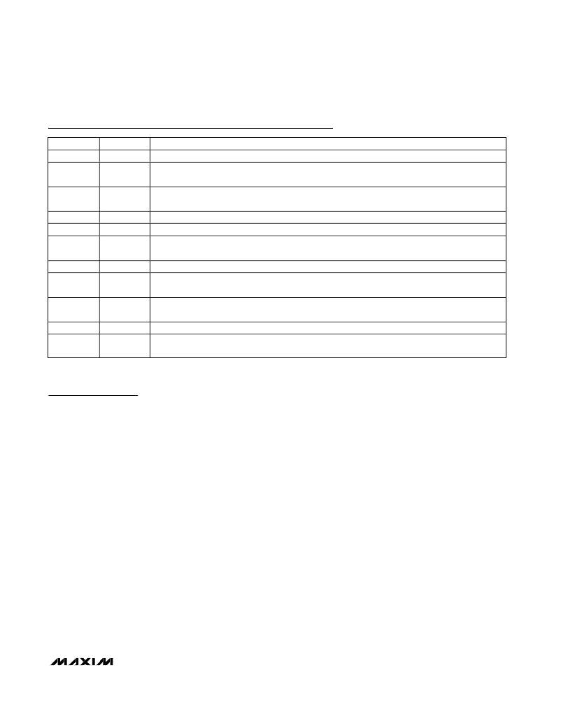
�Pin� Description� (continued)�
�PIN�
�14�
�15�
�16�
�17�
�18�
�19�
�20�
�21�
�22�
�23�
�24�
�NAME�
�DH1�
�LX1�
�BST1�
�DL1�
�PGND�
�V� L�
�DL2�
�BST2�
�LX2�
�DH2�
�EN�
�FUNCTION�
�High-Side� Gate� Driver� Output� for� Regulator� 1� (REG1).� DH1� swings� from� LX1� to� BST1.�
�External� Inductor� Connection� for� Regulator� 1� (REG1).� Connect� LX1� to� the� switched� side� of� the�
�inductor.� LX1� serves� as� the� lower� supply� rail� for� the� DH1� high-side� gate� driver.�
�Boost� Flying-Capacitor� Connection� for� Regulator� 1� (REG1).� Connect� BST1� to� an� external� ceramic�
�capacitor� and� diode� according� to� Figure� 1.�
�Low-Side� Gate-Driver� Output� for� Regulator� 1� (REG1).� DL1� swings� from� PGND� to� V� L� .�
�Power� Ground�
�Internal� 5V� Linear-Regulator� Output.� Supplies� the� regulators� and� powers� the� low-side� gate� drivers�
�and� external� boost� circuitry� for� the� high-side� gate� drivers.�
�Low-Side� Gate-Driver� Output� for� Regulator� 2� (REG2).� DL2� swings� from� PGND� to� V� L� .�
�Boost� Flying-Capacitor� Connection� for� Regulator� 2� (REG2).� Connect� BST2� to� an� external� ceramic�
�capacitor� and� diode� according� to� Figure� 1.�
�External� Inductor� Connection� for� Regulator� 2� (REG2).� Connect� LX2� to� the� switched� side� of� the�
�inductor.� LX2� serves� as� the� lower� supply� rail� for� the� DH2� high-side� gate� driver.�
�High-Side� Gate-Driver� Output� for� Regulator� 2� (REG2).� DH2� swings� from� LX2� to� BST2.�
�Active-High� Enable� Input.� A� logic� low� shuts� down� both� controllers.� Connect� to� V� L� for� always-on�
�operation.�
�Detailed� Description�
�DC-DC� PWM� Controller�
�The� MAX1858� step-down� converters� use� a� PWM� volt-�
�age-mode� control� scheme� (Figure� 2)� for� each� out-of-�
�phase� controller.� The� controller� generates� the� clock�
�signal� by� dividing� down� the� internal� oscillator� or� SYNC�
�input� when� driven� by� an� external� clock,� so� each� con-�
�troller� ’� s� switching� frequency� equals� half� the� oscillator�
�frequency� (f� SW� =� f� OSC� /2).� An� internal� transconductance�
�error� amplifier� produces� an� integrated� error� voltage� at�
�the� COMP� pin,� providing� high� DC� accuracy.� The� volt-�
�age� at� COMP� sets� the� duty� cycle� using� a� PWM� com-�
�parator� and� a� ramp� generator.� At� each� rising� edge� of�
�the� clock,� REG1� ’� s� high-side� N-channel� MOSFET� turns�
�on� and� remains� on� until� either� the� appropriate� duty�
�cycle� or� until� the� maximum� duty� cycle� is� reached.�
�REG2� operates� out-of-phase,� so� the� second� high-side�
�MOSFET� turns� on� at� each� falling� edge� of� the� clock.�
�During� each� high-side� MOSFET� ’� s� on-time,� the� associat-�
�ed� inductor� current� ramps� up.�
�During� the� second-half� of� the� switching� cycle,� the� high-�
�side� MOSFET� turns� off� and� the� low-side� N-channel�
�MOSFET� turns� on.� Now� the� inductor� releases� the� stored�
�energy� as� its� current� ramps� down,� providing� current� to�
�the� output.� Under� overload� conditions,� when� the� induc-�
�tor� current� exceeds� the� selected� valley� current-limit�
�(see� the� Current-Limit� Circuit� (ILIM_)� section),� the� high-�
�side� MOSFET� does� not� turn� on� at� the� appropriate� clock�
�edge� and� the� low-side� MOSFET� remains� on� to� let� the�
�inductor� current� ramp� down.�
�Synchronized� Out-of-Phase� Operation�
�The� two� independent� regulators� in� the� MAX1858� oper-�
�ate� 180� °� out-of-phase� to� reduce� input� filtering� require-�
�ments,� reduce� electromagnetic� interference� (EMI),� and�
�improve� efficiency.� This� effectively� lowers� component�
�cost� and� saves� board� space,� making� the� MAX1858�
�ideal� for� cost-sensitive� applications.�
�Dual-switching� regulators� typically� operate� both� con-�
�trollers� in-phase,� and� turn� on� both� high-side� MOSFETs�
�at� the� same� time.� The� input� capacitor� must� then� sup-�
�port� the� instantaneous� current� requirements� of� both�
�controllers� simultaneously,� resulting� in� increased� ripple�
�voltage� and� current� when� compared� to� a� single� switch-�
�ing� regulator.� The� higher� RMS� ripple� current� lowers� effi-�
�ciency� due� to� power� loss� associated� with� the� input�
�capacitor� ’� s� effective� series� resistance� (ESR).� This� typi-�
�cally� requires� more� low-ESR� input� capacitors� in� parallel�
�to� minimize� input� voltage� ripple� and� ESR-related� loss-�
�es,� or� to� meet� the� necessary� ripple-current� rating.�
�_______________________________________________________________________________________�
�7�
�相关PDF资料 |
PDF描述 |
|---|---|
| MAX772ESA+ | IC REG CTRLR BST PWM 8-SOIC |
| MAX1744AUB+ | IC REG CTRLR BUCK PWM 10-UMAX |
| GBC30DRYN-S93 | CONN EDGECARD 60POS DIP .100 SLD |
| GBC35DRYI-S93 | CONN EDGECARD 70POS DIP .100 SLD |
| MAX1962EEP+ | IC REG CTRLR BUCK PWM VM 20-QSOP |
相关代理商/技术参数 |
参数描述 |
|---|---|
| MAX1858EEG+ | 功能描述:电压模式 PWM 控制器 Dual 180 Out Buck Controllers RoHS:否 制造商:Texas Instruments 输出端数量:1 拓扑结构:Buck 输出电压:34 V 输出电流: 开关频率: 工作电源电压:4.5 V to 5.5 V 电源电流:600 uA 最大工作温度:+ 125 C 最小工作温度:- 40 C 封装 / 箱体:WSON-8 封装:Reel |
| MAX1858EEG+T | 功能描述:电压模式 PWM 控制器 Dual 180 Out Buck Controllers RoHS:否 制造商:Texas Instruments 输出端数量:1 拓扑结构:Buck 输出电压:34 V 输出电流: 开关频率: 工作电源电压:4.5 V to 5.5 V 电源电流:600 uA 最大工作温度:+ 125 C 最小工作温度:- 40 C 封装 / 箱体:WSON-8 封装:Reel |
| MAX1858EEG-T | 功能描述:DC/DC 开关控制器 RoHS:否 制造商:Texas Instruments 输入电压:6 V to 100 V 开关频率: 输出电压:1.215 V to 80 V 输出电流:3.5 A 输出端数量:1 最大工作温度:+ 125 C 安装风格: 封装 / 箱体:CPAK |
| MAX1858EVKIT | 功能描述:DC/DC 开关控制器 Evaluation Kit for the MAX1858 MAX1875 MAX1876 RoHS:否 制造商:Texas Instruments 输入电压:6 V to 100 V 开关频率: 输出电压:1.215 V to 80 V 输出电流:3.5 A 输出端数量:1 最大工作温度:+ 125 C 安装风格: 封装 / 箱体:CPAK |
| MAX185ACNG | 功能描述:模数转换器 - ADC RoHS:否 制造商:Texas Instruments 通道数量:2 结构:Sigma-Delta 转换速率:125 SPs to 8 KSPs 分辨率:24 bit 输入类型:Differential 信噪比:107 dB 接口类型:SPI 工作电源电压:1.7 V to 3.6 V, 2.7 V to 5.25 V 最大工作温度:+ 85 C 安装风格:SMD/SMT 封装 / 箱体:VQFN-32 |
发布紧急采购,3分钟左右您将得到回复。