- 您现在的位置:买卖IC网 > PDF目录5134 > MAX1904EAI+T (Maxim Integrated Products)IC CNTRLR PWR SPLY LN 28-SSOP PDF资料下载
参数资料
| 型号: | MAX1904EAI+T |
| 厂商: | Maxim Integrated Products |
| 文件页数: | 10/33页 |
| 文件大小: | 0K |
| 描述: | IC CNTRLR PWR SPLY LN 28-SSOP |
| 产品培训模块: | Lead (SnPb) Finish for COTS Obsolescence Mitigation Program |
| 标准包装: | 2,000 |
| 应用: | 控制器,笔记本电脑电源系统 |
| 输入电压: | 4.2 V ~ 30 V |
| 输出数: | 4 |
| 输出电压: | 2.5 V ~ 5 V |
| 工作温度: | 0°C ~ 85°C |
| 安装类型: | 表面贴装 |
| 封装/外壳: | 28-SSOP(0.209",5.30mm 宽) |
| 供应商设备封装: | 28-SSOP |
| 包装: | 带卷 (TR) |
第1页第2页第3页第4页第5页第6页第7页第8页第9页当前第10页第11页第12页第13页第14页第15页第16页第17页第18页第19页第20页第21页第22页第23页第24页第25页第26页第27页第28页第29页第30页第31页第32页第33页
�� �
�
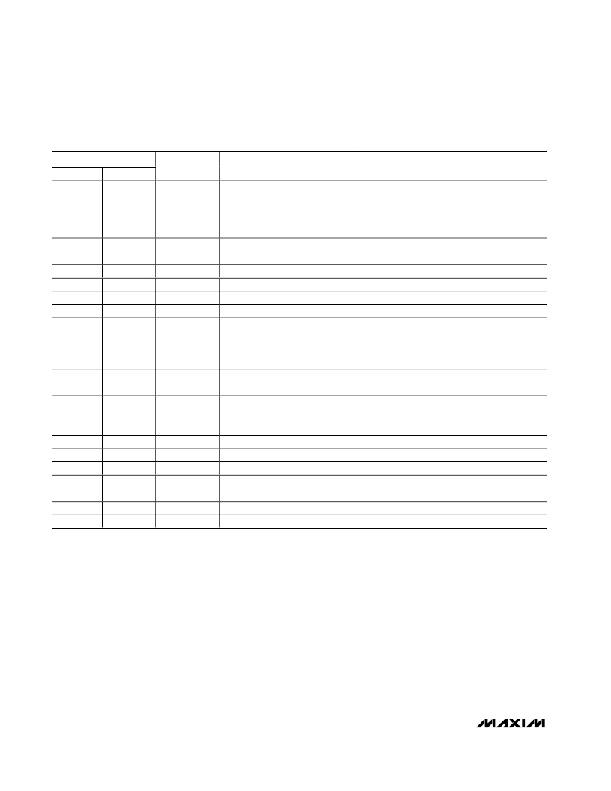
�500kHz� Multi-Output,� Low-Noise� Power-Supply�
�Controllers� for� Notebook� Computers�
�Pin� Description� (continued)�
�QSOP�
�PIN�
�QFN�
�NAME�
�FUNCTION�
�Pin-strap� input� that� selects� the� SMPS� power-up� sequence:�
�SEQ� =� GND:� 5V� before� 3.3V,� RESET� output� determined� by� both� outputs�
�15�
�13�
�SEQ�
�SEQ� =� REF:� Separate� ON3/ON5� controls,� RESET� output� determined� by� 3.3V�
�output�
�SEQ� =� V� L� :� 3.3V� before� 5V,� RESET� output� determined� by� both� outputs�
�16�
�17�
�18�
�19�
�20�
�14�
�15�
�17�
�18�
�19�
�DH5�
�LX5�
�BST5�
�DL5�
�PGND�
�Gate-Drive� Output� for� the� 5V,� High-Side� N-Channel� Switch.� DH5� is� a� floating� driver�
�output� that� swings� from� LX5� to� BST5,� riding� on� the� LX5� switching� node� voltage.�
�Switching-Node� (Inductor)� Connection.� Can� swing� 2V� below� ground� without� hazard.�
�Boost� Capacitor� Connection� for� High-Side� Gate� Drive� (0.1μF)�
�Gate-Drive� Output� for� the� Low-Side� Synchronous-Rectifier� MOSFET.� Swings� 0� to� V� L� .�
�Power� Ground�
�5V� Internal� Linear-Regulator� Output.� V� L� is� also� the� supply-voltage� rail� for� the� chip.�
�21�
�20�
�VL�
�After� the� 5V� SMPS� output� has� reached� 4.5V� (typ),� V� L� automatically� switches� to� the�
�output� voltage� through� CSL5� for� bootstrapping.� Bypass� to� GND� with� 4.7μF.� V� L�
�supplies� up� to� 25mA� for� external� loads.�
�22�
�21�
�V+�
�Battery� Voltage� Input,� 4.2V� to� 30V.� Bypass� V+� to� PGND� close� to� the� IC� with� a� 0.22μF�
�capacitor.� Connects� to� a� linear� regulator� that� powers� V� L� .�
�Shutdown� Control� Input,� Active� Low.� Logic� threshold� is� set� at� approximately� 1V.� For�
�23�
�22�
�SHDN�
�automatic� startup,� connect� SHDN� to� V+� through� a� 220k� ?� resistor� and� bypass� SHDN� to�
�GND� with� a� 0.01μF� capacitor.�
�24�
�25�
�26�
�27�
�28�
�—�
�23�
�24�
�26�
�27�
�28�
�6,� 16,� 25,� 32�
�DL3�
�BST3�
�LX3�
�DH3�
�RUN/ON3�
�N.C.�
�Gate-Drive� Output� for� the� Low-Side� Synchronous-Rectifier� MOSFET.� Swings� 0� to� VL.�
�Boost� Capacitor� Connection� for� High-Side� Gate� Drive� (0.1μF)�
�Switching-Node� (Inductor)� Connection.� Can� swing� 2V� below� ground� without� hazard.�
�Gate-Drive� Output� for� the� 3.3V,� High-Side� N-Channel� Switch.� DH3� is� a� floating� driver�
�output� that� swings� from� LX3� to� BST3,� riding� on� the� LX3� switching-node� voltage.�
�ON/� OFF� Control� Input.� See� the� Power-Up� Sequencing� and� ON/� OFF� Controls� section.�
�No� Connection�
�10�
�______________________________________________________________________________________�
�相关PDF资料 |
PDF描述 |
|---|---|
| MAX1902EAI+T | IC CNTRLR PWR SPLY LN 28-SSOP |
| UPM1A561MPD6 | CAP ALUM 560UF 10V 20% RADIAL |
| UPM1A561MPD | CAP ALUM 560UF 10V 20% RADIAL |
| MAX1901EAI+T | IC CNTRLR PWR SPLY LN 28-SSOP |
| UPM1A471MPD6 | CAP ALUM 470UF 10V 20% RADIAL |
相关代理商/技术参数 |
参数描述 |
|---|---|
| MAX1904EAI-TG074 | 制造商:Rochester Electronics LLC 功能描述: 制造商:Maxim Integrated Products 功能描述: |
| MAX1904ETJ | 功能描述:DC/DC 开关控制器 RoHS:否 制造商:Texas Instruments 输入电压:6 V to 100 V 开关频率: 输出电压:1.215 V to 80 V 输出电流:3.5 A 输出端数量:1 最大工作温度:+ 125 C 安装风格: 封装 / 箱体:CPAK |
| MAX1904ETJ+ | 功能描述:DC/DC 开关控制器 500kHz Multi-Output Power-Supply Ctlr RoHS:否 制造商:Texas Instruments 输入电压:6 V to 100 V 开关频率: 输出电压:1.215 V to 80 V 输出电流:3.5 A 输出端数量:1 最大工作温度:+ 125 C 安装风格: 封装 / 箱体:CPAK |
| MAX1904ETJ+T | 功能描述:DC/DC 开关控制器 500kHz Multi-Output Power-Supply Ctlr RoHS:否 制造商:Texas Instruments 输入电压:6 V to 100 V 开关频率: 输出电压:1.215 V to 80 V 输出电流:3.5 A 输出端数量:1 最大工作温度:+ 125 C 安装风格: 封装 / 箱体:CPAK |
| MAX1904ETJ-T | 功能描述:DC/DC 开关控制器 RoHS:否 制造商:Texas Instruments 输入电压:6 V to 100 V 开关频率: 输出电压:1.215 V to 80 V 输出电流:3.5 A 输出端数量:1 最大工作温度:+ 125 C 安装风格: 封装 / 箱体:CPAK |
发布紧急采购,3分钟左右您将得到回复。