- 您现在的位置:买卖IC网 > PDF目录18777 > MAX2160ETL+ (Maxim Integrated)IC TUNER ISDB-T LOW IF 40TQFN PDF资料下载
参数资料
| 型号: | MAX2160ETL+ |
| 厂商: | Maxim Integrated |
| 文件页数: | 21/25页 |
| 文件大小: | 0K |
| 描述: | IC TUNER ISDB-T LOW IF 40TQFN |
| 产品培训模块: | Lead (SnPb) Finish for COTS Obsolescence Mitigation Program |
| 标准包装: | 50 |
| 系列: | * |
| 频率: | 470MHz ~ 770MHz |
| 应用: | 手机 |
| 电流 - 接收: | 44mA |
| 数据接口: | PCB,表面贴装 |
| 存储容量: | * |
| 天线连接器: | PCB,表面贴装 |
| 电源电压: | 2.7 V ~ 3.3 V |
| 工作温度: | -40°C ~ 85°C |
| 封装/外壳: | 40-WFQFN 裸露焊盘 |
| 供应商设备封装: | 40-TQFN-EP(6x6) |
| 包装: | 托盘 |
�� �
�
�ISDB-T� Single-Segment� Low-IF� Tuners�
�Table� 16.� Typical� Supply� Current� Fluctuations� for� Nondefault� Register� Settings�
�MODE�
�Receive�
�Shutdown�
�Standby�
�Power-Down�
�BIT� CHANGE�
�Default� register� settings�
�QOFF� =� 1� (Q� channel� off)�
�BBL[1:0]� =� 00� (lower� linearity)�
�BBL[1:0]� =� 01� (nominal� linearity)�
�BBL[1:0]� =� 11� (high� linearity)�
�MOD� =� 1� (7dB� baseband� gain� step� enabled)�
�EPD� =� 1� (power� detector� enabled)�
�EPB� =� 0� (charge-pump� prebias� disabled)�
�XD[4:0]� =� 00000� (XTALOUT� buffer� disabled)�
�SHDN� =� GND�
�STBY� =� 1�
�PWDN� =� 1�
�TYPICAL� I� CC�
�46.5mA�
�—�
�—�
�—�
�—�
�—�
�—�
�—�
�—�
�1μA�
�2.2mA�
�13.5μA�
�TYPICAL� ?� I� CC� FROM�
�NOMINAL�
�—�
�-3.3mA�
�-2mA�
�-1mA�
�+1mA�
�+0.3mA�
�+1mA�
�+5.1mA�
�-40μA�
�—�
�—�
�—�
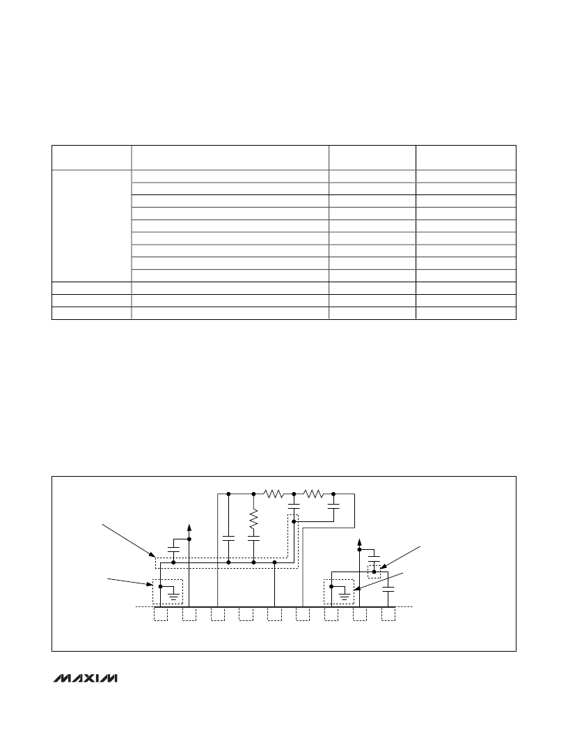
�Layout� Considerations�
�The� EV� kit� serves� as� a� guide� for� PC� board� layout.� Keep�
�RF� signal� lines� as� short� as� possible� to� minimize� losses�
�and� radiation.� Use� controlled� impedance� on� all� high-�
�frequency� traces.� For� proper� operation� of� the� TQFN�
�package,� the� exposed� paddle� must� be� soldered� evenly�
�to� the� board� ’s� ground� plane.� Use� abundant� vias�
�beneath� the� exposed� paddle� for� maximum� heat� dissi-�
�pation.� Use� abundant� ground� vias� between� RF� traces�
�to� minimize� undesired� coupling.� Bypass� each� V� CC� pin�
�to� ground� with� a� 100pF� capacitor� placed� as� close� to�
�the� pin� as� possible.�
�In� addition,� the� ground� returns� for� the� VCO,� VTUNE,�
�and� charge� pump� require� special� layout� consideration.�
�R21�
�The� VCOBYP� capacitor� (C37)� and� the� VCCVCO� bypass�
�capacitor� (C19)� ground� returns� must� be� routed� back� to�
�the� GNDVCO� pin� and� then� connected� to� the� overall�
�ground� plane� at� that� point� (GNDVCO).� All� loop� filter�
�component� grounds� (C27� –C30)� and� the� VCCCP�
�bypass� capacitor� (C17)� ground� must� all� be� routed�
�together� back� to� the� GNDCP� pin.� GNDTUNE� must� also�
�be� routed� back� to� the� GNDCP� pin� along� with� all� other�
�grounds� from� the� PLL� loop� filter.� The� GNDCP� pin� must�
�then� be� connected� to� the� overall� ground� plane.� Figure�
�4� shows� a� schematic� drawing� of� the� required� layout�
�connections.� Refer� to� the� MAX2160� evaluation� kit� for� a�
�recommended� board� layout.�
�R22�
�ROUTE� GNDTUNE,� C17,� AND� ALL�
�C29�
�C30�
�LOOP� FILTER� COMPONENT� GROUNDS� TO�
�GNDCP.�
�V� CC�
�R20�
�CONNECT� GNDCP� TO� THE� BOARD'S�
�GROUND� PLANE.�
�C17�
�C28�
�C27�
�V� CC�
�C19�
�ROUTE� C19� AND� C37� TO� GNDVCO.�
�CONNECT� GNDVCO� TO� THE� BOARD'S�
�GROUND� PLANE.�
�C37�
�40�
�39�
�38�
�37�
�36�
�35�
�34�
�33�
�32�
�Figure� 4.� Ground� Return� Layout� Connections� for� the� VCO,� Charge� Pump,� and� VTUNE�
�______________________________________________________________________________________�
�21�
�相关PDF资料 |
PDF描述 |
|---|---|
| MAX1471ATJ+ | IC RCVR ASK/FSK LP 32-TQFN |
| MICRF011BM | IC RCVR/DATA DEMOD RF/IF 14SOIC |
| AMB310908 | SENSOR REFL LONG H-TYPE |
| MICRF009BM | IC RECEIVER UHF LOW POWER 16SOIC |
| MICRF007BM | IC RECEIVER UHF LOW POWER 8SOIC |
相关代理商/技术参数 |
参数描述 |
|---|---|
| MAX2160ETL+ | 功能描述:调谐器 ISDB-T Single-Seg Low-IF Tuner RoHS:否 制造商:NXP Semiconductors 功能: 噪声系数: 工作电源电压: 最小工作温度: 最大工作温度: |
| MAX2160ETL+T | 功能描述:调谐器 ISDB-T Single-Seg Low-IF Tuner RoHS:否 制造商:NXP Semiconductors 功能: 噪声系数: 工作电源电压: 最小工作温度: 最大工作温度: |
| MAX2160ETL-T | 功能描述:调谐器 ISDB-T Single-Seg Low-IF Tuner RoHS:否 制造商:NXP Semiconductors 功能: 噪声系数: 工作电源电压: 最小工作温度: 最大工作温度: |
| MAX2160EVKIT | 功能描述:射频开发工具 MAX2160 Eval Kit RoHS:否 制造商:Taiyo Yuden 产品:Wireless Modules 类型:Wireless Audio 工具用于评估:WYSAAVDX7 频率: 工作电源电压:3.4 V to 5.5 V |
| MAX2161E/W-B3N | 功能描述:调谐器 RoHS:否 制造商:NXP Semiconductors 功能: 噪声系数: 工作电源电压: 最小工作温度: 最大工作温度: |
发布紧急采购,3分钟左右您将得到回复。