参数资料
| 型号: | MAX3676EHJ+ |
| 厂商: | Maxim Integrated Products |
| 文件页数: | 13/15页 |
| 文件大小: | 0K |
| 描述: | IC CLOCK RECOVERY 32-TQFP |
| 产品培训模块: | Lead (SnPb) Finish for COTS Obsolescence Mitigation Program |
| 标准包装: | 360 |
| 类型: | 时钟和数据恢复(CDR),多路复用器 |
| PLL: | 是 |
| 主要目的: | SONET/SDH |
| 输入: | PECL |
| 输出: | PECL |
| 电路数: | 1 |
| 比率 - 输入:输出: | 2:2 |
| 差分 - 输入:输出: | 是/是 |
| 频率 - 最大: | 622.08MHz |
| 电源电压: | 3 V ~ 5.5 V |
| 工作温度: | -40°C ~ 85°C |
| 安装类型: | 表面贴装 |
| 封装/外壳: | 32-TQFP |
| 供应商设备封装: | 32-TQFP(5x5) |
| 包装: | 托盘 |
MAX3676
622Mbps, 3.3V Clock-Recovery and
Data-Retiming IC with Limiting Amplifier
_______________________________________________________________________________________
7
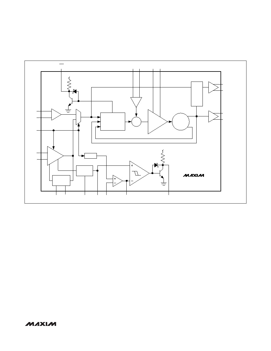
_______________Detailed Description
The block diagram in Figure 1 shows the MAX3676’s
architecture. It consists of a limiting-amplifier input
stage followed by a fully integrated clock/data-recovery
(CDR) block implemented with a PLL. The input stage
is selectable between a limiting amplifier or a simple
PECL input buffer. The limiting amplifier provides an
LOP monitor and an RSSI output. The PLL consists of a
phase/frequency detector (PFD), a loop filter amplifier,
and a voltage-controlled oscillator (VCO).
Limiting Amplifier
The MAX3676’s on-chip limiting amplifier accepts an
input signal level from 3.0mVP-P to 1.2VP-P. The amplifi-
er consists of a cascade of gain stages that include full-
wave logarithmic detectors. The combined small-signal
gain is approximately 42dB, and the -3dB bandwidth is
650MHz. Input-referred noise is typically 80μVRMS, pro-
viding excellent sensitivity for small-amplitude data
streams.
In addition to driving the CDR, the limiting amplifier pro-
vides both an RSSI output and an LOP monitor that
allow the user to program the threshold voltage. The
RSSI circuitry provides an output voltage that is linearly
proportional to the input power (in decibels) detected
between the ADI+ and ADI- input pins and is sensitive
enough to reliably detect signals as small as 2mVP-P
(see the
Typical Operating Characteristics).
Input DC offset reduces the accuracy of the power
detector; therefore, an integrated feedback loop is
included that automatically nulls the input offset of the
gain stage. The addition of this offset-correction loop
requires that the input signal be AC-coupled when
using the ADI+ and ADI- inputs.
Finally, for applications that do not require the limiting
amplifier, selecting the digital inputs conserves power
by turning off the postamplifier block.
MAX3676
LOL
PHASE/FREQ
DETECTOR
POWER
DETECT
OFFSET
CORRECTION
FILTER
622.08MHz
LIMITER
42dB
BIAS
VCO
Σ
DQ
Q
I
CFILT
RSSI
INV
VTH
LOP
FIL+ FIL-
PHADJ+
DDI+
DDI-
INSEL
ADI-
ADI+
PHADJ-
1.23V
SDO+
SDO-
PECL
VCC
6k
Ω
6k
Ω
PECL
SCLKO+
SCLKO-
OLC+
OLC-
Figure 1. Functional Diagram
相关PDF资料 |
PDF描述 |
|---|---|
| ADN2813ACPZ | IC CLK/DATA REC 1.25GBPS 48LFCSP |
| AD800-52BRZ | IC CLK\DATA RECOVERY PLL 20SOIC |
| SY87700VZH | IC CLK/DATA RECOVERY 3.3V 28SOIC |
| MS27467P25B35PC | CONN PLUG 128POS STRAIGHT W/PINS |
| AD9558BCPZ | IC CLOCK TRANSLATOR 64LFCSP |
相关代理商/技术参数 |
参数描述 |
|---|---|
| MAX3676EHJ+ | 功能描述:时钟发生器及支持产品 622Mbps 3.3V Clock Recovery RoHS:否 制造商:Silicon Labs 类型:Clock Generators 最大输入频率:14.318 MHz 最大输出频率:166 MHz 输出端数量:16 占空比 - 最大:55 % 工作电源电压:3.3 V 工作电源电流:1 mA 最大工作温度:+ 85 C 安装风格:SMD/SMT 封装 / 箱体:QFN-56 |
| MAX3676EHJ+T | 功能描述:时钟发生器及支持产品 622Mbps 3.3V Clock Recovery RoHS:否 制造商:Silicon Labs 类型:Clock Generators 最大输入频率:14.318 MHz 最大输出频率:166 MHz 输出端数量:16 占空比 - 最大:55 % 工作电源电压:3.3 V 工作电源电流:1 mA 最大工作温度:+ 85 C 安装风格:SMD/SMT 封装 / 箱体:QFN-56 |
| MAX3676EHJ-T | 功能描述:时钟发生器及支持产品 622Mbps 3.3V Clock Recovery RoHS:否 制造商:Silicon Labs 类型:Clock Generators 最大输入频率:14.318 MHz 最大输出频率:166 MHz 输出端数量:16 占空比 - 最大:55 % 工作电源电压:3.3 V 工作电源电流:1 mA 最大工作温度:+ 85 C 安装风格:SMD/SMT 封装 / 箱体:QFN-56 |
| MAX3677CTJ+ | 制造商:Microsemi Corporation 功能描述:+3.3V, LOW-JITTER CLOCK GEN W/MULT OUT - Trays 制造商:Microsemi Corporation 功能描述:Microsemi MAX3677CTJ+ Clocks - Timers 制造商:MICROSEMI CONSUMER MEDICAL PRODUCT GROUP 功能描述:IC CLOCK GENERATOR PROGR 32TQFN 制造商:Microsemi Corporation 功能描述:IC CLOCK GENERATOR PROGR 32TQFN |
| MAX3677CTJ+T | 制造商:Microsemi Corporation 功能描述:+3.3V, LOW-JITTER CLOCK GEN W/MULT OUT - Tape and Reel |
发布紧急采购,3分钟左右您将得到回复。