参数资料
| 型号: | MAX3676EHJ+ |
| 厂商: | Maxim Integrated Products |
| 文件页数: | 14/15页 |
| 文件大小: | 0K |
| 描述: | IC CLOCK RECOVERY 32-TQFP |
| 产品培训模块: | Lead (SnPb) Finish for COTS Obsolescence Mitigation Program |
| 标准包装: | 360 |
| 类型: | 时钟和数据恢复(CDR),多路复用器 |
| PLL: | 是 |
| 主要目的: | SONET/SDH |
| 输入: | PECL |
| 输出: | PECL |
| 电路数: | 1 |
| 比率 - 输入:输出: | 2:2 |
| 差分 - 输入:输出: | 是/是 |
| 频率 - 最大: | 622.08MHz |
| 电源电压: | 3 V ~ 5.5 V |
| 工作温度: | -40°C ~ 85°C |
| 安装类型: | 表面贴装 |
| 封装/外壳: | 32-TQFP |
| 供应商设备封装: | 32-TQFP(5x5) |
| 包装: | 托盘 |
MAX3676
622Mbps, 3.3V Clock-Recovery and
Data-Retiming IC with Limiting Amplifier
8
_______________________________________________________________________________________
Phase Detector
The phase detector produces a voltage proportional to
the phase difference between the incoming data and
the internal clock. Because of its feedback nature, the
PLL drives the error voltage to zero, aligning the recov-
ered clock to the incoming data. The external phase
adjustment pins (PHADJ+, PHADJ-) allow the user to
vary the internal phase alignment.
Frequency Detector
The frequency detector incorporated into the PLL uses
the input data stream edges to sample the quadrature
components of the VCO clock. This generates a differ-
ence frequency that aids acquisition during startup.
Depending on the polarity of the difference frequency,
the PFD drives the VCO so that the difference frequen-
cy is reduced to zero. Once frequency acquisition is
obtained, the frequency detector returns to a neutral
state.
Loop Filter and VCO
The VCO is fully integrated, while the loop filter requires
an external capacitor (CF). This filter network determines
the bandwidth and peaking of the second-order PLL.
__________________Design Procedure
Received-Signal-Strength Indicator
The RSSI output voltage is insensitive to temperature
and supply fluctuations. The power detector functions
as a broadband power meter that detects the total RMS
power of all signals within the detector bandwidth
(including input signal noise). The RSSI voltage varies
linearly (in decibels) for inputs of 2mVP-P to 50mVP-P.
The slope over this input range is approximately
26mV/dB.
The high-speed RSSI signal is filtered to an RMS level
with one external capacitor tied from CFILT to VCC. The
impedance looking into CFILT is about 500
Ω to VCC. As
a result, the lower -3dB cutoff frequency is set by the
following simple relationship:
fFILT = 1/[2
π(500)CFILT]
For 622Mbps applications, Maxim recommends a cut-
off frequency of 6.8kHz, which requires CFILT = 47nF.
The RSSI output is designed to drive a minimum load
resistance of 100k
Ω to ground and a maximum of
20pF. Loads greater than 20pF must be buffered by a
series resistance of 100k
Ω (i.e., voltmeter).
Input Offset Correction
The on-chip limiting amplifier provides more than 42dB
of gain. A low-frequency feedback loop is integrated
into the MAX3676 to remove the input offset. DC-cou-
pling to the ADI+ and ADI- inputs is not allowed, as this
would prevent the proper functioning of the DC offset-
correction circuitry.
The differential input impedance (ZIN) is approximately
2.5k
Ω. The impedance between OLC+ and OLC- (ZOLC)
is approximately 120k
Ω. Take care when setting the
combined low-frequency cutoff (fCUTOFF), due to the
input DC-blocking capacitor (CIN) and the offset correc-
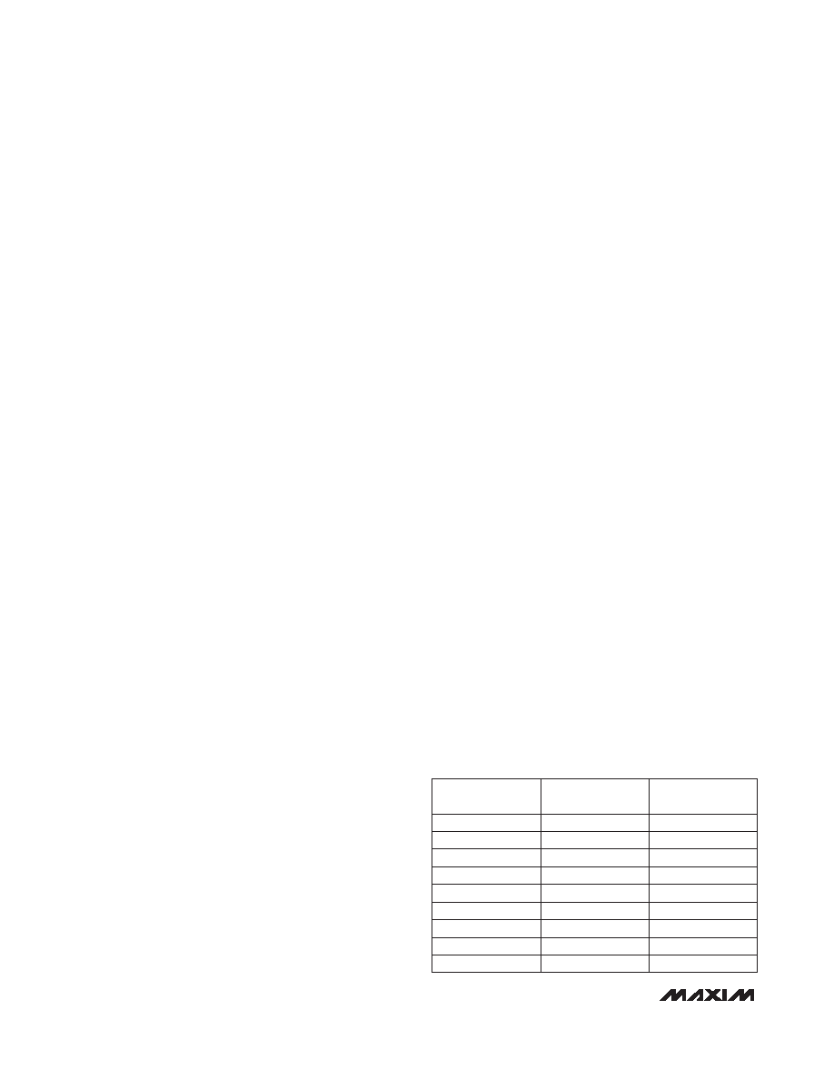
tion loop capacitor (COLC). See Table 1 for selecting the
values of CIN and COLC.
These values ensure that the poles associated with CIN
and COLC work together to provide a flat response at the
lower -3dB corner frequency (no gain peaking).
CIN must be a low-TC, high-quality capacitor of type X7R
or better in order to minimize fCUTOFF deviations. COLC
must be a capacitor of type Z5U or better.
Loss-of-Power Monitor
An LOP monitor with a user-programmable threshold
and a hysteresis comparator is also included with the
limiting amplifier circuitry. Internally, one comparator
input is tied to the RSSI output signal, and the other is
tied to the threshold voltage (VTH), which is set exter-
nally and provides a trip point for the LOP indication. A
low-voltage, low-drift op amp, referenced to an internal
bandgap voltage (1.23V), is supplied for programming
a supply independent threshold voltage. This op amp
requires two external resistors to program the LOP trip
point. VTH is programmable from 1.23V to 2.6V using
the equation:
VTH = 1.23(1 + R2/R1)
The op amp can source only 100μA of current.
Therefore, an R1 value of 20k
Ω is recommended for
proper operation. The input bias current of the op amp
at the INV pin is less than ±100nA.
COLC
COMBINED LOW
fCUTOFF (kHz)
2200pF
0.015μF
29
1000pF
0.01μF
68
CIN
470pF
3300pF
135
330pF
2200pF
190
220pF
1500pF
290
Table 1. Setting the Low-Frequency Cutoff
4700pF
0.033μF
13.5
6800pF
0.082μF
10
0.010μF
0.1μF
6.8
0.022μF
0.15μF
3.0
相关PDF资料 |
PDF描述 |
|---|---|
| ADN2813ACPZ | IC CLK/DATA REC 1.25GBPS 48LFCSP |
| AD800-52BRZ | IC CLK\DATA RECOVERY PLL 20SOIC |
| SY87700VZH | IC CLK/DATA RECOVERY 3.3V 28SOIC |
| MS27467P25B35PC | CONN PLUG 128POS STRAIGHT W/PINS |
| AD9558BCPZ | IC CLOCK TRANSLATOR 64LFCSP |
相关代理商/技术参数 |
参数描述 |
|---|---|
| MAX3676EHJ+ | 功能描述:时钟发生器及支持产品 622Mbps 3.3V Clock Recovery RoHS:否 制造商:Silicon Labs 类型:Clock Generators 最大输入频率:14.318 MHz 最大输出频率:166 MHz 输出端数量:16 占空比 - 最大:55 % 工作电源电压:3.3 V 工作电源电流:1 mA 最大工作温度:+ 85 C 安装风格:SMD/SMT 封装 / 箱体:QFN-56 |
| MAX3676EHJ+T | 功能描述:时钟发生器及支持产品 622Mbps 3.3V Clock Recovery RoHS:否 制造商:Silicon Labs 类型:Clock Generators 最大输入频率:14.318 MHz 最大输出频率:166 MHz 输出端数量:16 占空比 - 最大:55 % 工作电源电压:3.3 V 工作电源电流:1 mA 最大工作温度:+ 85 C 安装风格:SMD/SMT 封装 / 箱体:QFN-56 |
| MAX3676EHJ-T | 功能描述:时钟发生器及支持产品 622Mbps 3.3V Clock Recovery RoHS:否 制造商:Silicon Labs 类型:Clock Generators 最大输入频率:14.318 MHz 最大输出频率:166 MHz 输出端数量:16 占空比 - 最大:55 % 工作电源电压:3.3 V 工作电源电流:1 mA 最大工作温度:+ 85 C 安装风格:SMD/SMT 封装 / 箱体:QFN-56 |
| MAX3677CTJ+ | 制造商:Microsemi Corporation 功能描述:+3.3V, LOW-JITTER CLOCK GEN W/MULT OUT - Trays 制造商:Microsemi Corporation 功能描述:Microsemi MAX3677CTJ+ Clocks - Timers 制造商:MICROSEMI CONSUMER MEDICAL PRODUCT GROUP 功能描述:IC CLOCK GENERATOR PROGR 32TQFN 制造商:Microsemi Corporation 功能描述:IC CLOCK GENERATOR PROGR 32TQFN |
| MAX3677CTJ+T | 制造商:Microsemi Corporation 功能描述:+3.3V, LOW-JITTER CLOCK GEN W/MULT OUT - Tape and Reel |
发布紧急采购,3分钟左右您将得到回复。