- 您现在的位置:买卖IC网 > PDF目录17280 > MAX5066EVKIT (Maxim Integrated Products)EVAL KIT FOR MAX5066 PDF资料下载
参数资料
| 型号: | MAX5066EVKIT |
| 厂商: | Maxim Integrated Products |
| 文件页数: | 8/22页 |
| 文件大小: | 0K |
| 描述: | EVAL KIT FOR MAX5066 |
| 产品培训模块: | Lead (SnPb) Finish for COTS Obsolescence Mitigation Program |
| 标准包装: | 1 |
| 主要目的: | DC/DC,步降 |
| 输出及类型: | 2,非隔离 |
| 输出电压: | 0.8V,1.3V |
| 电流 - 输出: | 10A,10A |
| 输入电压: | 5 ~ 16 V |
| 稳压器拓扑结构: | 降压 |
| 频率 - 开关: | 500kHz |
| 板类型: | 完全填充 |
| 已供物品: | 板 |
| 已用 IC / 零件: | MAX5066 |
�� �
�
�Configurable,� Single-/Dual-Output,� Synchronous�
�Buck� Controller� for� High-Current� Applications�
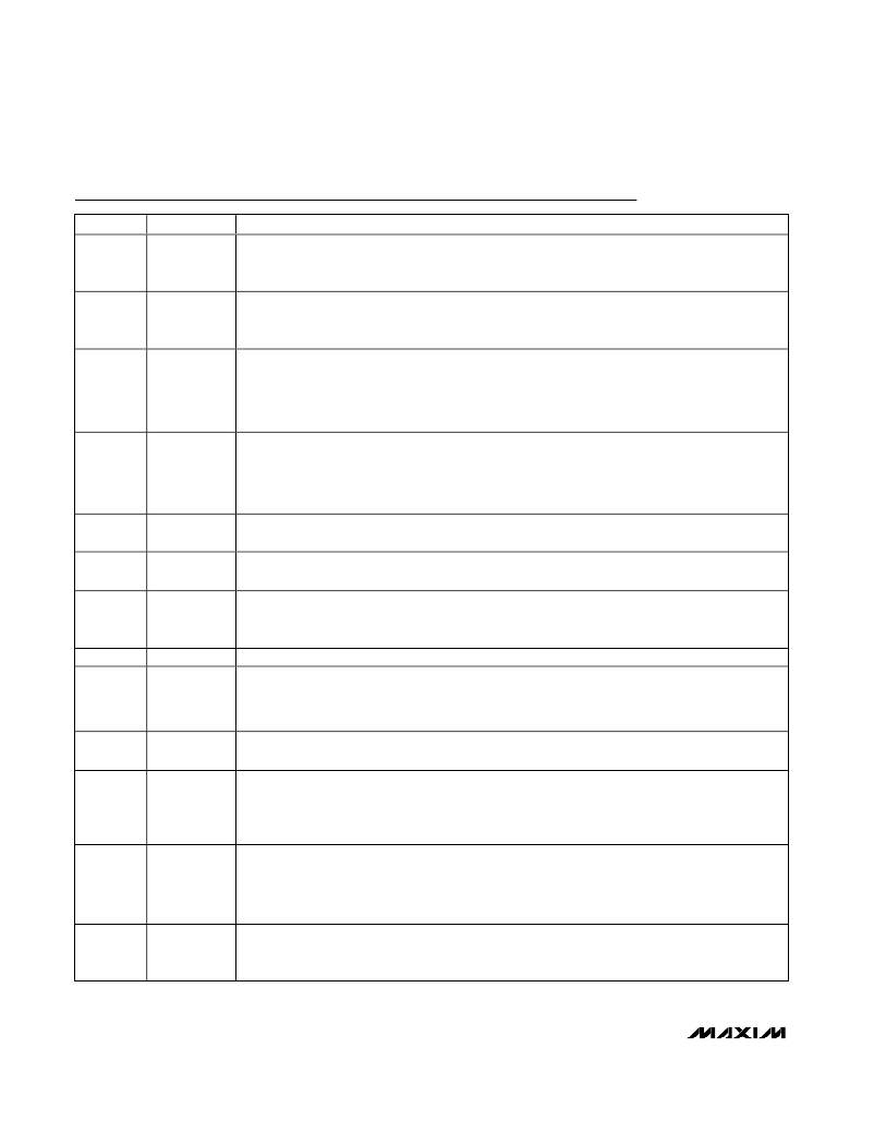
�Pin� Description�
�PIN�
�1�
�2�
�3�
�4�
�5�
�6�
�7�
�8�
�9�
�10�
�11�
�12�
�13�
�NAME�
�CSN2�
�CSP2�
�EAOUT2�
�EAN2�
�CLP2�
�REF�
�RT/CLKIN�
�AGND�
�MODE�
�CLP1�
�EAN1�
�EAOUT1�
�CSP1�
�FUNCTION�
�Current-Sense� Differential� Amplifier� Negative� Input� for� Output2.� Connect� CSN2� to� the� negative�
�terminal� of� the� sense� resistor.� The� differential� voltage� between� CSP2� and� CSN2� is� internally� amplified�
�by� the� current-sense� amplifier� (A� V(CS)� =� 36V/V).�
�Current-Sense� Differential� Amplifier� Positive� Input� for� Output2.� Connect� CSP2� to� the� positive� terminal�
�of� the� sense� resistor.� The� differential� voltage� between� CSP2� and� CSN2� is� internally� amplified� by� the�
�current-sense� amplifier� (A� V(CS)� =� 36V/V).�
�Voltage� Error-Amplifier� Output2.� Connect� to� an� external� gain-setting� feedback� resistor.� The� error-�
�amplifier� gain� determines� the� output� voltage� load� regulation� for� adaptive� voltage� positioning.� This�
�output� also� serves� as� the� compensation� network� connection� from� EAOUT2� to� EAN2.� A� resistive�
�network� results� in� a� drooped� output� voltage� regulation� characteristic.� An� integrator� configuration�
�results� in� very� tight� output� voltage� regulation� (see� the� Adaptive� Voltage� Positioning� section).�
�Voltage� Error-Amplifier� Inverting� Input� for� Output2.� Connect� a� resistive� divider� from� V� OUT2� to� EAN2� to�
�AGND� to� set� the� output� voltage.� A� compensation� network� connects� from� EAOUT2� to� EAN2.� A�
�resistive� network� results� in� a� drooped� output-voltage-regulation� characteristic.� An� integrator�
�configuration� results� in� very� tight� output-voltage� regulation� (see� the� Adaptive� Voltage� Positioning�
�section).�
�Current-Error� Amplifier� Output2.� Compensate� the� current� loop� by� connecting� an� R-C� network� from�
�CLP2� to� AGND.�
�3.3V� Reference� Output.� Bypass� REF� to� AGND� with� a� minimum� 0.1μF� ceramic� capacitor.� REF� can�
�source� up� to� 200μA� for� external� loads.�
�External� Clock� Input� or� Internal� Frequency-Setting� Connection.� Connect� a� resistor� from� RT/CLKIN� to�
�AGND� to� set� the� switching� frequency.� Connect� an� external� clock� at� RT/CLKIN� for� external� frequency�
�synchronization.�
�Analog� Ground�
�Mode� Function� Input.� MODE� selects� between� a� single-output� dual� phase� or� a� dual-output� buck�
�regulator.� When� MODE� is� grounded,� VEA1� and� VEA2� connect� to� CEA1� and� CEA2,� respectively� (see�
�Figure� 1)� and� the� device� operates� as� a� two-output,� out-of-phase� buck� regulator.� When� MODE� is�
�connected� to� REG� (logic� high),� VEA2� is� disconnected� and� VEA1� is� routed� to� both� CEA1� and� CEA2.�
�Current-Error� Amplifier� Output1.� Compensate� the� current� loop� by� connecting� an� R-C� network� from�
�CLP1� to� AGND.�
�Voltage� Error� Amplifier� Inverting� Input� for� Output1.� Connect� a� resistive� divider� from� V� OUT1� to� EAN1� to�
�regulate� the� output� voltage.� A� compensation� network� connects� from� EAOUT1� to� EAN1.� A� resistive�
�network� results� in� a� drooped� output-voltage-regulation� characteristic.� An� integrator� configuration�
�results� in� very� tight� output� voltage� regulation� (see� the� Adaptive� Voltage� Positioning� section).�
�Voltage� Error� Amplifier� Output1.� Connect� to� an� external� gain-setting� feedback� resistor.� The� error�
�amplifier� gain� determines� the� output-voltage-load� regulation� for� adaptive� voltage� positioning.� This�
�output� also� serves� as� the� compensation� network� connection� from� EAOUT1� to� EAN1.� A� resistive�
�network� results� in� a� drooped� output-voltage-regulation� characteristic.� An� integrator� configuration�
�results� in� very� tight� output-voltage� regulation� (see� the� Adaptive� Voltage� Positioning� section).�
�Current-Sense� Differential� Amplifier� Positive� Input� for� Output1.� Connect� CSP1� to� the� positive� terminal�
�of� the� sense� resistor.� The� differential� voltage� between� CSP1� and� CSN1� is� internally� amplified� by� the�
�current-sense� amplifier� (A� V(CS)� =� 36V/V).�
�8�
�_______________________________________________________________________________________�
�相关PDF资料 |
PDF描述 |
|---|---|
| L-14C27NJV4T | CER INDUCTOR 27NH 0603 |
| MC33385VW | IC SWITCH QUAD L-SIDE 20-HSOP |
| MC33186VW1 | IC DRIVER H-BRIDGE 20-HSOP |
| ASEK712ELC-30A-T-DK | BOARD EVAL FOR ASEK712ELC-30A |
| L-14C82NJV4T | CER INDUCTOR 82NH 0603 |
相关代理商/技术参数 |
参数描述 |
|---|---|
| MAX5067 | 制造商:MAXIM 制造商全称:Maxim Integrated Products 功能描述:Dual-Phase, +0.6V to +3.3V Output Parallelable, Average-Current-Mode Controllers |
| MAX5067ETH | 功能描述:电流型 PWM 控制器 Dual-Phase .6-3.3V Parallelable Average RoHS:否 制造商:Texas Instruments 开关频率:27 KHz 上升时间: 下降时间: 工作电源电压:6 V to 15 V 工作电源电流:1.5 mA 输出端数量:1 最大工作温度:+ 105 C 安装风格:SMD/SMT 封装 / 箱体:TSSOP-14 |
| MAX5067ETH+ | 功能描述:电流型 PWM 控制器 Dual-Phase .6-3.3V Parallelable Average RoHS:否 制造商:Texas Instruments 开关频率:27 KHz 上升时间: 下降时间: 工作电源电压:6 V to 15 V 工作电源电流:1.5 mA 输出端数量:1 最大工作温度:+ 105 C 安装风格:SMD/SMT 封装 / 箱体:TSSOP-14 |
| MAX5067ETH+T | 功能描述:电流型 PWM 控制器 Dual-Phase .6-3.3V Parallelable Average RoHS:否 制造商:Texas Instruments 开关频率:27 KHz 上升时间: 下降时间: 工作电源电压:6 V to 15 V 工作电源电流:1.5 mA 输出端数量:1 最大工作温度:+ 105 C 安装风格:SMD/SMT 封装 / 箱体:TSSOP-14 |
| MAX5067ETH-T | 功能描述:电流型 PWM 控制器 Dual-Phase .6-3.3V Parallelable Average RoHS:否 制造商:Texas Instruments 开关频率:27 KHz 上升时间: 下降时间: 工作电源电压:6 V to 15 V 工作电源电流:1.5 mA 输出端数量:1 最大工作温度:+ 105 C 安装风格:SMD/SMT 封装 / 箱体:TSSOP-14 |
发布紧急采购,3分钟左右您将得到回复。