- 您现在的位置:买卖IC网 > PDF目录17280 > MAX5066EVKIT (Maxim Integrated Products)EVAL KIT FOR MAX5066 PDF资料下载
参数资料
| 型号: | MAX5066EVKIT |
| 厂商: | Maxim Integrated Products |
| 文件页数: | 9/22页 |
| 文件大小: | 0K |
| 描述: | EVAL KIT FOR MAX5066 |
| 产品培训模块: | Lead (SnPb) Finish for COTS Obsolescence Mitigation Program |
| 标准包装: | 1 |
| 主要目的: | DC/DC,步降 |
| 输出及类型: | 2,非隔离 |
| 输出电压: | 0.8V,1.3V |
| 电流 - 输出: | 10A,10A |
| 输入电压: | 5 ~ 16 V |
| 稳压器拓扑结构: | 降压 |
| 频率 - 开关: | 500kHz |
| 板类型: | 完全填充 |
| 已供物品: | 板 |
| 已用 IC / 零件: | MAX5066 |
�� �
�
�Configurable,� Single-/Dual-Output,� Synchronous�
�Buck� Controller� for� High-Current� Applications�
�Pin� Description� (continued)�
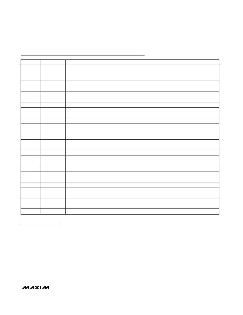
�PIN�
�14�
�15�
�16�
�17�
�18�
�19�
�20�
�21�
�22�
�23�
�24�
�25�
�26�
�27�
�28�
�EP�
�NAME�
�CSN1�
�EN1�
�BST1�
�DH1�
�LX1�
�DL1�
�V� DD�
�REG�
�IN�
�PGND�
�DL2�
�LX2�
�DH2�
�BST2�
�EN2�
�EP�
�FUNCTION�
�Current-Sense� Differential� Amplifier� Negative� Input� for� Output1.� Connect� CSN1� to� the� negative�
�terminal� of� the� sense� resistor.� The� differential� voltage� between� CSP1� and� CSN1� is� internally� amplified�
�by� the� current-sense� amplifier� (A� V(CS)� =� 36V/V).�
�Output� 1� Enable.� A� logic-low� shuts� down� channel� 1’s� MOSFET� drivers.� EN1� can� be� used� for� output�
�sequencing.�
�Boost� Flying� Capacitor� Connection.� Reservoir� capacitor� connection� for� the� high-side� MOSFET� driver�
�supply.� Connect� a� 0.47μF� ceramic� capacitor� between� BST1� and� LX1.�
�High-Side� Gate� Driver� Output1.� DH1� drives� the� gate� of� the� high-side� MOSFET.�
�External� inductor� connection� and� source� connection� for� the� high-side� MOSFET� for� Output1.� LX1� also�
�serves� as� the� return� terminal� for� the� high-side� MOSFET� driver.�
�Low-Side� Gate� Driver� Output1.� Gate� driver� output� for� the� synchronous� MOSFET.�
�Supply� Voltage� for� Low-Side� Drivers.� REG� powers� V� DD� .� Connect� a� parallel� combination� of� 0.1μF� and�
�1μF� ceramic� capacitors� from� V� DD� to� PGND� and� a� 1� ?� resistor� from� V� DD� to� REG� to� filter� out� the� high-�
�peak� currents� of� the� driver� from� the� internal� circuitry.�
�Internal� 5V� Regulator� Output.� REG� is� derived� internally� from� IN� and� is� used� to� power� the� internal� bias�
�circuitry.� Bypass� REG� to� AGND� with� a� 4.7μF� ceramic� capacitor.�
�Supply� Voltage� Connection.� Connect� IN� to� a� 5V� to� 28V� input� supply.�
�Power� Ground.� Source� connection� for� the� low-side� MOSFET.� Connect� V� DD� ’s� bypass� capacitor� returns�
�to� PGND.�
�Low-Side� Gate� Driver� Output2.� Gate� driver� for� the� synchronous� MOSFET.�
�External� inductor� connection� and� source� connection� for� the� high-side� MOSFET� for� Output2.� Also�
�serves� as� the� return� terminal� for� the� high-side� MOSFET� driver.�
�High-Side� Gate� Driver� Output2.� DH2� drives� the� gate� of� the� high-side� MOSFET.�
�Boost� Flying� Capacitor� Connection.� Reservoir� capacitor� connection� for� the� high-side� MOSFET� driver�
�supply.� Connect� a� 0.47μF� ceramic� capacitor� between� BST2� and� LX2.�
�Output� 2� Enable.� A� logic-low� shuts� down� channel� 2’s� MOSFET� drivers.� EN2� can� be� used� for� output�
�sequencing.�
�Exposed� Pad.� Connect� exposed� pad� to� ground� plane.�
�Detailed� Description�
�The� MAX5066� switching� power-supply� controller� can�
�be� configured� in� two� ways.� With� the� MODE� input� high,� it�
�operates� as� a� single-output,� dual-phase,� step-down�
�switching� regulator� where� each� output� is� 180°� out� of�
�phase.� With� the� MODE� pin� connected� low,� the�
�MAX5066� operates� as� a� dual-output,� step-down� switch-�
�ing� regulator.� The� average� current-mode� control� topolo-�
�gy� of� the� MAX5066� offers� high-noise� immunity� while�
�having� benefits� similar� to� those� of� peak� current-mode�
�control.� Average� current-mode� control� has� the� intrinsic�
�ability� to� accurately� limit� the� average� current� sourced�
�by� the� converter� during� a� fault� condition.� When� a� fault�
�condition� occurs,� the� error� amplifier� output� voltage�
�(EAOUT1� or� EAOUT2)� that� connects� to� the� positive�
�input� of� the� transconductance� amplifier� (CA1� or� CA2)� is�
�clamped� thus� limiting� the� output� current.�
�The� MAX5066� contains� all� blocks� necessary� for� two�
�independently� regulated� average� current-mode� PWM�
�regulators.� It� has� two� voltage� error� amplifiers� (VEA1�
�and� VEA2),� two� current-error� amplifiers� (CEA1� and�
�CEA2),� two� current-sensing� amplifiers� (CA1� and� CA2),�
�two� PWM� comparators� (CPWM1� and� CPWM2),� and� dri-�
�vers� for� both� low-� and� high-side� power� MOSFETs� (see�
�Figure� 1).� Each� PWM� section� is� also� equipped� with� a�
�pulse-by-pulse,� current-limit� protection� and� a� fault� inte-�
�gration� block� for� hiccup� protection.�
�_______________________________________________________________________________________�
�9�
�相关PDF资料 |
PDF描述 |
|---|---|
| L-14C27NJV4T | CER INDUCTOR 27NH 0603 |
| MC33385VW | IC SWITCH QUAD L-SIDE 20-HSOP |
| MC33186VW1 | IC DRIVER H-BRIDGE 20-HSOP |
| ASEK712ELC-30A-T-DK | BOARD EVAL FOR ASEK712ELC-30A |
| L-14C82NJV4T | CER INDUCTOR 82NH 0603 |
相关代理商/技术参数 |
参数描述 |
|---|---|
| MAX5067 | 制造商:MAXIM 制造商全称:Maxim Integrated Products 功能描述:Dual-Phase, +0.6V to +3.3V Output Parallelable, Average-Current-Mode Controllers |
| MAX5067ETH | 功能描述:电流型 PWM 控制器 Dual-Phase .6-3.3V Parallelable Average RoHS:否 制造商:Texas Instruments 开关频率:27 KHz 上升时间: 下降时间: 工作电源电压:6 V to 15 V 工作电源电流:1.5 mA 输出端数量:1 最大工作温度:+ 105 C 安装风格:SMD/SMT 封装 / 箱体:TSSOP-14 |
| MAX5067ETH+ | 功能描述:电流型 PWM 控制器 Dual-Phase .6-3.3V Parallelable Average RoHS:否 制造商:Texas Instruments 开关频率:27 KHz 上升时间: 下降时间: 工作电源电压:6 V to 15 V 工作电源电流:1.5 mA 输出端数量:1 最大工作温度:+ 105 C 安装风格:SMD/SMT 封装 / 箱体:TSSOP-14 |
| MAX5067ETH+T | 功能描述:电流型 PWM 控制器 Dual-Phase .6-3.3V Parallelable Average RoHS:否 制造商:Texas Instruments 开关频率:27 KHz 上升时间: 下降时间: 工作电源电压:6 V to 15 V 工作电源电流:1.5 mA 输出端数量:1 最大工作温度:+ 105 C 安装风格:SMD/SMT 封装 / 箱体:TSSOP-14 |
| MAX5067ETH-T | 功能描述:电流型 PWM 控制器 Dual-Phase .6-3.3V Parallelable Average RoHS:否 制造商:Texas Instruments 开关频率:27 KHz 上升时间: 下降时间: 工作电源电压:6 V to 15 V 工作电源电流:1.5 mA 输出端数量:1 最大工作温度:+ 105 C 安装风格:SMD/SMT 封装 / 箱体:TSSOP-14 |
发布紧急采购,3分钟左右您将得到回复。