- 您现在的位置:买卖IC网 > PDF目录10739 > MAX5863ETM+ (Maxim Integrated Products)IC AFE 8/10BIT 7.5MSPS 48-TQFN PDF资料下载
参数资料
| 型号: | MAX5863ETM+ |
| 厂商: | Maxim Integrated Products |
| 文件页数: | 7/26页 |
| 文件大小: | 0K |
| 描述: | IC AFE 8/10BIT 7.5MSPS 48-TQFN |
| 产品培训模块: | Lead (SnPb) Finish for COTS Obsolescence Mitigation Program |
| 标准包装: | 43 |
| 位数: | 8,10 |
| 通道数: | 8 |
| 功率(瓦特): | 22.8mW |
| 电压 - 电源,模拟: | 2.7 V ~ 3.3 V |
| 电压 - 电源,数字: | 1.8 V ~ 3.3 V |
| 封装/外壳: | 48-WFQFN 裸露焊盘 |
| 供应商设备封装: | 48-TQFN-EP(7x7) |
| 包装: | 管件 |
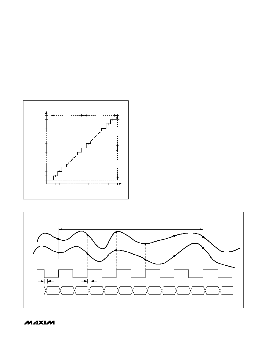
ADC System Timing Requirements
Figure 3 shows the relationship between the clock, ana-
log inputs, and the resulting output data. Channel IA
(CHI) and channel QA (CHQ) are simultaneously sam-
pled on the rising edge of the clock signal (CLK) and
the resulting data is multiplexed at the DA0–DA7 out-
puts. CHI data is updated on the rising edge and CHQ
data is updated on the falling edge of the CLK.
Including the delay through the output latch, the total
clock-cycle latency is 5 clock cycles for CHI and 5.5
clock cycles for CHQ.
Dual 10-Bit DAC
The 10-bit DACs are capable of operating with clock
speeds up to 7.5MHz. The DAC’s digital inputs,
DD0–DD9, are multiplexed on a single 10-bit bus. The
voltage reference determines the data converters’ full-
scale output voltages. See the Reference Configurations
section for setting reference voltage. The DACs utilize a
current-array technique with a 1mA (with 1.024V refer-
ence) full-scale output current driving a 400
internal
resistor resulting in a
±400mV full-scale differential out-
put voltage. The MAX5863 is designed for differential
output only and is not intended for single-ended appli-
cation. The analog outputs are biased at 1.4V common
mode and designed to drive a differential input stage
with input impedance
≥70k. This simplifies the analog
interface between RF quadrature upconverters and the
MAX5863. RF upconverters require a 1.3V to 1.5V com-
mon-mode bias. The internal DC common-mode bias
eliminates discrete level-setting resistors and code-gen-
erated level-shifting while preserving the full dynamic
range of each transmit DAC. Table 2 shows the output
voltage vs. input code.
MAX5863
Ultra-Low-Power, High-Dynamic
Performance, 7.5Msps Analog Front End
______________________________________________________________________________________
15
Figure 3. ADC System Timing Diagram
tDOQ
tDOI
5 CLOCK-CYCLE LATENCY (CHI), 5.5 CLOCK-CYCLE LATENCY (CHQ)
DA0–DA7
D0Q
D1I
D1Q
D2I
D2Q
D3I
D3Q
D4I
D4Q
D5I
D5Q
D6I
D6Q
CHI
CHQ
CLK
Figure 2. ADC Transfer Function
INPUT VOLTAGE (LSB)
-1
-126 -125
256
2 x VREF
1 LSB =
VREF = VREFP - VREFN
VREF
V
REF
V
REF
0+1
-127
+126
+128
+127
-128
+125
(COM)
OFFSET
BINAR
Y
OUTPUT
CODE
(LSB)
0000 0000
0000 0001
0000 0010
0000 0011
1111 1111
1111 1110
1111 1101
0111 1111
1000 0000
1000 0001
相关PDF资料 |
PDF描述 |
|---|---|
| VI-23L-IW | CONVERTER MOD DC/DC 28V 100W |
| VI-23K-IW | CONVERTER MOD DC/DC 40V 100W |
| VI-23J-IW | CONVERTER MOD DC/DC 36V 100W |
| VI-23H-IW | CONVERTER MOD DC/DC 52V 100W |
| VI-23D-IW | CONVERTER MOD DC/DC 85V 100W |
相关代理商/技术参数 |
参数描述 |
|---|---|
| MAX5863ETM+ | 功能描述:ADC / DAC多通道 10-Bit 2Ch 7.5Msps CODEC/AFE RoHS:否 制造商:Texas Instruments 转换速率: 分辨率:8 bit 接口类型:SPI 电压参考: 电源电压-最大:3.6 V 电源电压-最小:2 V 最大工作温度:+ 85 C 安装风格:SMD/SMT 封装 / 箱体:VQFN-40 |
| MAX5863ETM+T | 功能描述:ADC / DAC多通道 RoHS:否 制造商:Texas Instruments 转换速率: 分辨率:8 bit 接口类型:SPI 电压参考: 电源电压-最大:3.6 V 电源电压-最小:2 V 最大工作温度:+ 85 C 安装风格:SMD/SMT 封装 / 箱体:VQFN-40 |
| MAX5863ETM-T | 功能描述:ADC / DAC多通道 RoHS:否 制造商:Texas Instruments 转换速率: 分辨率:8 bit 接口类型:SPI 电压参考: 电源电压-最大:3.6 V 电源电压-最小:2 V 最大工作温度:+ 85 C 安装风格:SMD/SMT 封装 / 箱体:VQFN-40 |
| MAX5864ETM | 功能描述:ADC / DAC多通道 RoHS:否 制造商:Texas Instruments 转换速率: 分辨率:8 bit 接口类型:SPI 电压参考: 电源电压-最大:3.6 V 电源电压-最小:2 V 最大工作温度:+ 85 C 安装风格:SMD/SMT 封装 / 箱体:VQFN-40 |
| MAX5864ETM+ | 功能描述:ADC / DAC多通道 10-Bit 2Ch 22Msps CODEC/AFE RoHS:否 制造商:Texas Instruments 转换速率: 分辨率:8 bit 接口类型:SPI 电压参考: 电源电压-最大:3.6 V 电源电压-最小:2 V 最大工作温度:+ 85 C 安装风格:SMD/SMT 封装 / 箱体:VQFN-40 |
发布紧急采购,3分钟左右您将得到回复。