- 您现在的位置:买卖IC网 > PDF目录10739 > MAX5863ETM+ (Maxim Integrated Products)IC AFE 8/10BIT 7.5MSPS 48-TQFN PDF资料下载
参数资料
| 型号: | MAX5863ETM+ |
| 厂商: | Maxim Integrated Products |
| 文件页数: | 9/26页 |
| 文件大小: | 0K |
| 描述: | IC AFE 8/10BIT 7.5MSPS 48-TQFN |
| 产品培训模块: | Lead (SnPb) Finish for COTS Obsolescence Mitigation Program |
| 标准包装: | 43 |
| 位数: | 8,10 |
| 通道数: | 8 |
| 功率(瓦特): | 22.8mW |
| 电压 - 电源,模拟: | 2.7 V ~ 3.3 V |
| 电压 - 电源,数字: | 1.8 V ~ 3.3 V |
| 封装/外壳: | 48-WFQFN 裸露焊盘 |
| 供应商设备封装: | 48-TQFN-EP(7x7) |
| 包装: | 管件 |
Shutdown mode offers the most dramatic power sav-
ings by shutting down all the analog sections of the
MAX5863 and placing the ADCs’ digital outputs in tri-
state mode. When the ADCs’ outputs transition from tri-
state to on, the last converted word is placed on the
digital outputs. The DACs’ digital bus inputs must be
zero or OVDD because the bus is not internally pulled
up. The DACs’ previously stored data is lost when com-
ing out of shutdown mode. The wake-up time from shut-
down mode is dominated by the time required to
charge the capacitors at REFP, REFN, and COM. In
internal reference mode and buffered external refer-
ence mode, the wake-up time is typically 40s to enter
Xcvr mode, 20s to enter RX mode, and 40s to enter
TX mode.
In idle mode, the reference and clock distribution cir-
cuits are powered, but all other functions are off. The
ADCs’ outputs are forced to tri-state. The DACs’ digital
bus inputs must be zero or OVDD, because the bus is
not internally pulled up. The wake-up time from the idle
mode is 10s required for the ADCs and DACs to be
fully operational. When the ADCs’ outputs transition
from tri-state to on, the last converted word is placed
on the digital outputs. In the idle mode, the supply cur-
rent is lowered if the clock input is set to zero or OVDD;
however, the wake-up time extends to 40s.
In standby mode, only the ADCs’ reference is powered;
the rest of the device’s functions are off. The pipeline
ADCs are off and DA0 to DA7 are in tri-state mode. The
DACs’ digital bus inputs must be zero or OVDD
because the bus is not internally pulled up. The wake-
up time from standby mode to the Xcvr mode is domi-
nated by the 40s required to activate the pipeline
ADCs and DACs. When the ADC outputs transition from
tri-state to active, the last converted word is placed on
the digital outputs.
The serial digital interface is a standard 3-wire connec-
tion compatible with SPI/QSPI/MICROWIRE/DSP
interfaces. Set CS low to enable the serial data loading
at DIN. Following CS high-to-low transition, data is shift-
ed synchronously, MSB first, on the rising edge of the
serial clock (SCLK). After 8 bits are loaded into the seri-
al input register, data is transferred to the latch. CS
must transition high for a minimum of 80ns before the
next write sequence. The SCLK can idle either high or
low between transitions. Figure 5 shows the detailed
timing diagram of the 3-wire serial interface.
MAX5863
Ultra-Low-Power, High-Dynamic
Performance, 7.5Msps Analog Front End
______________________________________________________________________________________
17
QSPI is a trademark of Motorola, Inc.
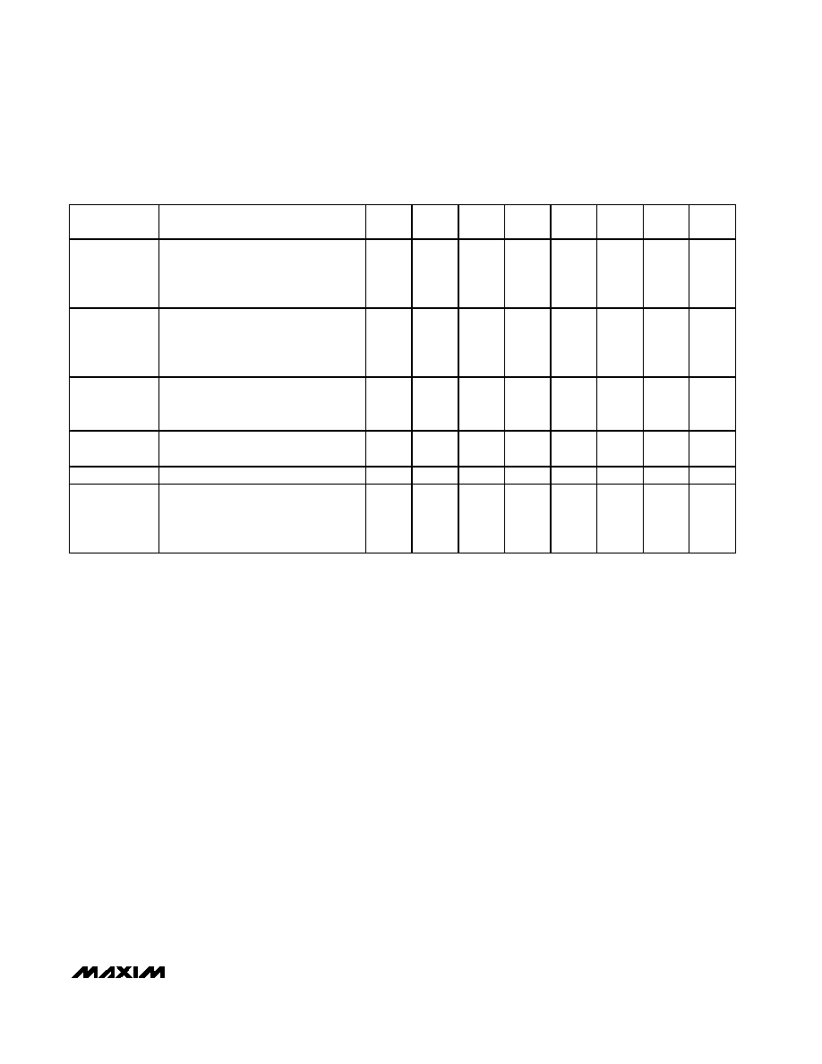
Table 3. MAX5863 Operation Modes
FUNCTION
DESCRIPTION
D7
(MSB)
D6
D5
D4
D3
D2
D1
D0
Shutdown
Device shutdown. REF is off, ADCs are
off, and the ADC bus is tri-stated; DACs
are off and the DAC input bus must be
set to zero or OVDD.
XX
X
0
Idle
REF and CLK are on, ADCs are off,
and the ADC bus is tri-stated; DACs
are off and the DAC input bus must be
set to zero or OVDD.
XX
X
0
1
RX
REF is on, ADCs are on; DACs are off,
and the DAC input bus must be set to
zero or OVDD.
XX
X
0
1
0
TX
REF is on, ADCs are off, and the ADC
bus is tri-stated; DACs are on.
XX
X
0
1
Xcvr
REF is on, ADCs and DACs are on.
X
1
0
Standby
REF is on, ADCs are off, and the ADC
bus is tri-stated; DACs are off and the
DAC input bus must be set to zero or
OVDD.
XX
X
1
0
1
x = Don’t care.
相关PDF资料 |
PDF描述 |
|---|---|
| VI-23L-IW | CONVERTER MOD DC/DC 28V 100W |
| VI-23K-IW | CONVERTER MOD DC/DC 40V 100W |
| VI-23J-IW | CONVERTER MOD DC/DC 36V 100W |
| VI-23H-IW | CONVERTER MOD DC/DC 52V 100W |
| VI-23D-IW | CONVERTER MOD DC/DC 85V 100W |
相关代理商/技术参数 |
参数描述 |
|---|---|
| MAX5863ETM+ | 功能描述:ADC / DAC多通道 10-Bit 2Ch 7.5Msps CODEC/AFE RoHS:否 制造商:Texas Instruments 转换速率: 分辨率:8 bit 接口类型:SPI 电压参考: 电源电压-最大:3.6 V 电源电压-最小:2 V 最大工作温度:+ 85 C 安装风格:SMD/SMT 封装 / 箱体:VQFN-40 |
| MAX5863ETM+T | 功能描述:ADC / DAC多通道 RoHS:否 制造商:Texas Instruments 转换速率: 分辨率:8 bit 接口类型:SPI 电压参考: 电源电压-最大:3.6 V 电源电压-最小:2 V 最大工作温度:+ 85 C 安装风格:SMD/SMT 封装 / 箱体:VQFN-40 |
| MAX5863ETM-T | 功能描述:ADC / DAC多通道 RoHS:否 制造商:Texas Instruments 转换速率: 分辨率:8 bit 接口类型:SPI 电压参考: 电源电压-最大:3.6 V 电源电压-最小:2 V 最大工作温度:+ 85 C 安装风格:SMD/SMT 封装 / 箱体:VQFN-40 |
| MAX5864ETM | 功能描述:ADC / DAC多通道 RoHS:否 制造商:Texas Instruments 转换速率: 分辨率:8 bit 接口类型:SPI 电压参考: 电源电压-最大:3.6 V 电源电压-最小:2 V 最大工作温度:+ 85 C 安装风格:SMD/SMT 封装 / 箱体:VQFN-40 |
| MAX5864ETM+ | 功能描述:ADC / DAC多通道 10-Bit 2Ch 22Msps CODEC/AFE RoHS:否 制造商:Texas Instruments 转换速率: 分辨率:8 bit 接口类型:SPI 电压参考: 电源电压-最大:3.6 V 电源电压-最小:2 V 最大工作温度:+ 85 C 安装风格:SMD/SMT 封装 / 箱体:VQFN-40 |
发布紧急采购,3分钟左右您将得到回复。