- 您现在的位置:买卖IC网 > PDF目录1849 > MAX8744AETJ+T (Maxim Integrated Products)IC CNTRLR PWR SUP QUAD 32TQFN PDF资料下载
参数资料
| 型号: | MAX8744AETJ+T |
| 厂商: | Maxim Integrated Products |
| 文件页数: | 23/36页 |
| 文件大小: | 0K |
| 描述: | IC CNTRLR PWR SUP QUAD 32TQFN |
| 标准包装: | 2,500 |
| 应用: | 控制器,笔记本电脑电源系统 |
| 输入电压: | 6 V ~ 26 V |
| 输出数: | 4 |
| 输出电压: | 3.3V,5V,1 V ~ 26 V |
| 工作温度: | 0°C ~ 85°C |
| 安装类型: | 表面贴装 |
| 封装/外壳: | 32-WFQFN 裸露焊盘 |
| 供应商设备封装: | 32-TQFN-EP(5x5) |
| 包装: | 带卷 (TR) |
第1页第2页第3页第4页第5页第6页第7页第8页第9页第10页第11页第12页第13页第14页第15页第16页第17页第18页第19页第20页第21页第22页当前第23页第24页第25页第26页第27页第28页第29页第30页第31页第32页第33页第34页第35页第36页
�� �
�
�High-Efficiency,� Quad-Output,� Main� Power-�
�Supply� Controllers� for� Notebook� Computers�
�V� GS� (� TH� )� >� V� IN� ?� RSS� ?�
�In forced-PWM mode, the MAX8744A/MAX8745A also�
�implement� a� negative� current� limit� to� prevent� excessive�
�reverse� inductor� currents� when� V� OUT� is� sinking� current.�
�The� negative� current-limit� threshold� is� set� to� approxi-�
�mately� 120%� of� the� positive� current� limit� and� tracks� the�
�positive� current� limit� when� ILIM� is� adjusted.�
�Connect� ILIM� to� LDO5� for� the� 50mV� default� threshold,�
�or� adjust� the� current-limit� threshold� with� an� external�
�resistor-divider� at� ILIM.� Use� a� 2μA� to� 20μA� divider� cur-�
�rent� for� accuracy� and� noise� immunity.� The� current-limit�
�threshold� adjustment� range� is� from� 50mV� to� 200mV.� In�
�the� adjustable� mode,� the� current-limit� threshold� voltage�
�equals� precisely� 1/10� the� voltage� seen� at� ILIM.� The�
�logic� threshold� for� switchover� to� the� default� value� is�
�approximately� V� LDO5� -� 1V.�
�Carefully� observe� the� PCB� layout� guidelines� to� ensure�
�that� noise� and� DC� errors� do� not� corrupt� the� differential�
�current-sense� signals� seen� by� CSH_� and� CSL_.� Place�
�the� IC� close� to� the� sense� resistor� with� short,� direct�
�traces,� making� a� Kelvin-sense� connection� to� the� cur-�
�rent-sense� resistor.�
�MOSFET� Gate� Drivers� (DH_,� DL_)�
�The� DH_� and� DL_� drivers� are� optimized� for� driving�
�moderate-sized� high-side� and� larger� low-side� power�
�MOSFETs.� This� is� consistent� with� the� low� duty� factor�
�seen� in� notebook� applications,� where� a� large� V� IN� -�
�V� OUT� differential� exists.� The� high-side� gate� drivers�
�(DH_)� source� and� sink� 2A,� and� the� low-side� gate� dri-�
�vers� (DL_)� source� 1.7A� and� sink� 3.3A.� This� ensures�
�robust� gate� drive� for� high-current� applications.� The�
�DH_� floating� high-side� MOSFET� drivers� are� powered� by�
�Applications� with� high� input� voltages� and� long� inductive�
�driver� traces� may� require� additional� gate-to-source�
�capacitance� to� ensure� fast-rising� LX_� edges� do� not� pull�
�up� the� low-side� MOSFETs� gate,� causing� shoot-through�
�currents.� The� capacitive� coupling� between� LX_� and� DL_�
�created� by� the� MOSFET’s� gate-to-drain� capacitance�
�(C� GD� =� C� RSS� ),� gate-to-source� capacitance� (C� GS� =� C� ISS�
�-� C� GD� ),� and� additional� board� parasitics� should� not�
�exceed� the� following� minimum� threshold:�
�?� C� ?�
�?� C� ISS� ?�
�Lot-to-lot� variation� of� the� threshold� voltage� may� cause�
�problems� in� marginal� designs.�
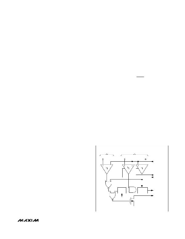
�Power-Good� Output� (PGOOD_)�
�PGOOD_� is� the� open-drain� output� of� a� comparator� that�
�continuously� monitors� both� SMPS� output� voltages� and�
�the� auxiliary� LDO� output� for� undervoltage� conditions.�
�PGOOD_� is� actively� held� low� in� shutdown� (� SHDN� =�
�GND),� standby� (ON3� =� ON5� =� ONA� =� GND),� soft-start,�
�and� soft-shutdown.� Once� the� soft-start� sequence� termi-�
�nates,� PGOOD_� becomes� high� impedance� as� long� as�
�the� outputs� are� above� 90%� of� the� nominal� regulation� volt-�
�age� set� by� FB_.� PGOOD_� goes� low� once� the� respective�
�output� drops� 10%� below� its� nominal� regulation� point,� an�
�SMPS� output� overvoltage� fault� occurs,� or� ON_� or� SHDN�
�is� low.� For� a� logic-level� PGOOD_� output� voltage,� connect�
�an� external� pullup� resistor� between� PGOOD_� and� LDO5.�
�A� 100k� Ω� pullup� resistor� works� well� in� most� applications.�
�charge� pumps� at� BST_� while� the� DL_� synchronous-rec-�
�tifier� drivers� are� powered� directly� by� the� fixed� 5V� linear�
�regulator� (LDO5).�
�POWER-GOOD�
�FAULT�
�PROTECTION�
�Adaptive� dead-time� circuits� monitor� the� DL_� and� DH_�
�drivers� and� prevent� either� FET� from� turning� on� until� the�
�0.9� x� INT� REF_�
�0.7� x� INT� REF_�
�1.11� x� INT� REF_�
�INTERNAL� FB�
�other� is� fully� off.� The� adaptive� driver� dead-time� allows�
�operation� without� shoot-through� with� a� wide� range� of�
�MOSFETs,� minimizing� delays� and� maintaining� efficiency.�
�There� must� be� a� low-resistance,� low-inductance� path�
�from� the� DL_� and� DH_� drivers� to� the� MOSFET� gates� for�
�the� adaptive� dead-time� circuits� to� work� properly;� other-�
�wise,� the� sense� circuitry� in� the� MAX8744A/MAX8745A�
�ENABLE� OVP�
�ENABLE� UVP�
�interprets� the� MOSFET� gates� as� “off”� while� charge� actu-�
�ally� remains.� Use� very� short,� wide� traces� (50� mils� to� 100�
�6144�
�CLK�
�FAULT�
�LATCH�
�FAULT�
�mils� wide� if� the� MOSFET� is� 1in� from� the� driver).�
�The� internal� pulldown� transistor� that� drives� DL_� low� is�
�robust,� with� a� 0.6� Ω� (typ)� on-resistance.� This� helps� prevent�
�DL_� from� being� pulled� up� due� to� capacitive� coupling� from�
�the� drain� to� the� gate� of� the� low-side� MOSFETs� when� the�
�inductor� node� (LX_)� quickly� switches� from� ground� to� V� IN� .�
�POR�
�Figure� 6.� Power-Good� and� Fault� Protection�
�POWER-GOOD�
�______________________________________________________________________________________�
�23�
�相关PDF资料 |
PDF描述 |
|---|---|
| MAX8745ETJ+ | IC CNTRLR PWR SUP QUAD 32TQFN |
| MAX8751ETJ+T | IC CNTRLR CCFL INV 32-TQFN |
| MAX8752ETA+T | IC DC-DC CONV TFT LCD 8-TDFN |
| MAX8753ETI+T | IC DC-DC CONV TFT LCD 28TQFN |
| MAX8756ETI+T | IC CNTRL DUAL PS 28-TQFN |
相关代理商/技术参数 |
参数描述 |
|---|---|
| MAX8744AEVKIT+ | 制造商:Maxim Integrated Products 功能描述:MAX8744A EVAL KIT - Rail/Tube |
| MAX8744ETJ+ | 功能描述:电流型 PWM 控制器 Quad-Out Main Power Supply Controller RoHS:否 制造商:Texas Instruments 开关频率:27 KHz 上升时间: 下降时间: 工作电源电压:6 V to 15 V 工作电源电流:1.5 mA 输出端数量:1 最大工作温度:+ 105 C 安装风格:SMD/SMT 封装 / 箱体:TSSOP-14 |
| MAX8744ETJ+T | 功能描述:电流和电力监控器、调节器 Quad-Out Main Power Supply Controller RoHS:否 制造商:STMicroelectronics 产品:Current Regulators 电源电压-最大:48 V 电源电压-最小:5.5 V 工作温度范围:- 40 C to + 150 C 安装风格:SMD/SMT 封装 / 箱体:HPSO-8 封装:Reel |
| MAX8744EVKIT | 制造商:Maxim Integrated Products 功能描述:HIGH-EFFICIENCY QUAD OUTPUT MAIN - Rail/Tube |
| MAX8744EVKIT+ | 制造商:Maxim Integrated Products 功能描述:HIGH-EFFICIENCY QUAD OUTPUT MAIN - Rail/Tube |
发布紧急采购,3分钟左右您将得到回复。