- 您现在的位置:买卖IC网 > PDF目录16560 > MAX8819CETI+T (Maxim Integrated Products)IC PMIC W/INT CHARGER 28TQFN-EP PDF资料下载
参数资料
| 型号: | MAX8819CETI+T |
| 厂商: | Maxim Integrated Products |
| 文件页数: | 14/29页 |
| 文件大小: | 0K |
| 描述: | IC PMIC W/INT CHARGER 28TQFN-EP |
| 产品培训模块: | Lead (SnPb) Finish for COTS Obsolescence Mitigation Program |
| 标准包装: | 2,500 |
| 应用: | 手持/移动设备 |
| 电源电压: | 4.1 V ~ 5.5 V |
| 工作温度: | -40°C ~ 85°C |
| 安装类型: | 表面贴装 |
| 封装/外壳: | 28-WFQFN 裸露焊盘 |
| 供应商设备封装: | 28-TQFN-EP(4x4) |
| 包装: | 带卷 (TR) |
第1页第2页第3页第4页第5页第6页第7页第8页第9页第10页第11页第12页第13页当前第14页第15页第16页第17页第18页第19页第20页第21页第22页第23页第24页第25页第26页第27页第28页第29页
�� �
�
�PMIC� with� Integrated� Chargers� and� Smart�
�Power� Selector� in� a� 4mm� x� 4mm� TQFN�
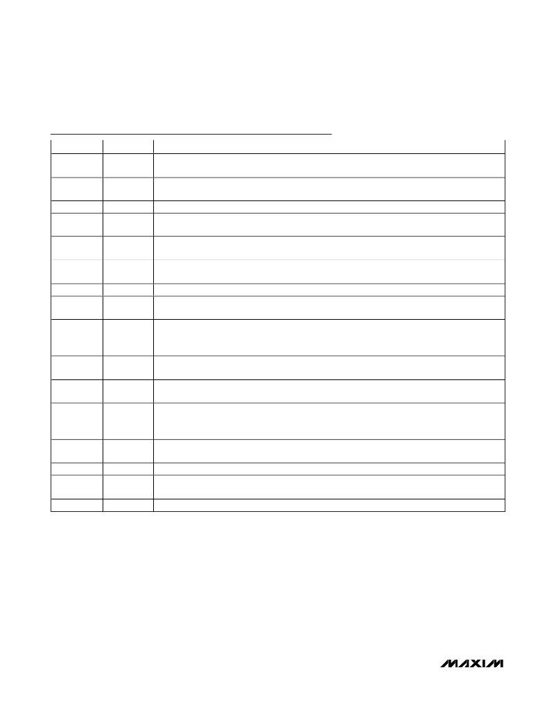
�Pin� Description� (continued)�
�PIN�
�14�
�15�
�16�
�17�
�18�
�19�
�20�
�21�
�22�
�23�
�24�
�25�
�26�
�27�
�28�
�—�
�NAME�
�CISET�
�CHG�
�PG1�
�LX1�
�PV13�
�LX3�
�PG3�
�DLIM1�
�FB2�
�FB3�
�EN123�
�PV2�
�LX2�
�PG2�
�DLIM2�
�EP�
�FUNCTION�
�Charge� Rate� Select� Input.� Connect� a� resistor� from� CISET� to� GND� (R� CISET� )� to� set� the� fast-charge�
�current� limit,� prequalification-charge� current� limit,� and� top-off� threshold.�
�Active-Low,� Open-Drain� Charge� Status� Output.� CHG� pulls� low� to� indicate� that� the� battery� is� charging.�
�See� Figure� 3� for� more� information.�
�REG1� Power� Ground�
�Inductor� Switching� Node� for� REG1.� When� enabled,� LX1� switches� between� PV13� and� PG1� to� regulate�
�the� FB1� voltage� to� 1.0V.� When� disabled,� LX1� is� pulled� to� PG1� by� 1k� Ω� in� shutdown.�
�Power� Input� for� the� REG1� and� REG3� Converters.� Connect� PV13� to� SYS.� Bypass� PV13� to� PG1� with� a�
�4.7μF� ceramic� capacitor.�
�Inductor� Switching� Node� for� REG3.� When� enabled,� LX3� switches� between� PV13� and� PG3� to� regulate�
�the� FB3� voltage� to� 1.0V.� When� disabled,� LX3� is� pulled� to� PG3� by� a� 1k� Ω� internal� resistor.�
�REG3� Power� Ground�
�Input� Current-Limit� Selection� Digital� Input� 1.� Drive� high� or� low� according� to� Table� 1� to� set� the� DC� input�
�current� limit.�
�Feedback� Input� for� REG2.� Connect� FB2� to� the� center� of� a� resistor� voltage-divider� from� the� REG2�
�output� capacitors� to� GND� to� set� the� output� voltage� from� 1V� to� V� SYS� .� FB2� must� be� connected� to� GND� if�
�REG2� is� disabled� by� grounding� PV2.�
�Feedback� Input� for� REG3.� Connect� FB3� to� the� center� of� a� resistor� voltage-divider� from� the� REG3�
�output� capacitors� to� GND� to� set� the� output� voltage� from� 1V� to� V� SYS� .�
�REG1,� REG2,� and� REG3� Enable� Input.� Drive� EN123� high� to� enable� REG1,� REG2,� and� REG3.� Drive� EN123�
�low� to� disable� REG1,� REG2,� and� REG3.� The� enable/disable� sequencing� is� shown� in� Figures� 6� and� 7.�
�Power� Input� for� REG2.� Connect� PV2� to� SYS� for� normal� operation.� Bypass� PV2� to� PG2� with� a� 2.2μF�
�ceramic� capacitor.� For� systems� that� do� not� require� REG2,� connect� PV2,� FB2,� and� PG2� to� GND� (LX2�
�may� be� unconnected� or� connected� to� GND).�
�Inductor� Switching� Node� for� REG2.� When� enabled,� LX2� switches� between� PV2� and� PG2� to� regulate�
�the� FB2� voltage� to� 1.0V.� When� disabled,� LX2� is� pulled� to� PG2� by� a� 1k� Ω� internal� resistor.�
�REG2� Power� Ground�
�Input� Current-Limit� Selection� Digital� Input� 2.� Drive� high� or� low� according� to� Table� 1� to� set� the� DC� input�
�current� limit.�
�Exposed� Pad�
�14�
�______________________________________________________________________________________�
�相关PDF资料 |
PDF描述 |
|---|---|
| MAX749ESA+T | IC SUPPLY LCD BIAS ADJ 8-SOIC |
| RSA06DRSN-S288 | CONN EDGECARD 12POS .125 EXTEND |
| H3CCS-6406M | IDC CABLE - HKC64S/AE64M/HKC64S |
| UPC3218GV-EVAL | EVAL BOARD FOR UPC3218GV |
| M2MXH-2020K | IDC CABLE - MDM20H/MC20F/X |
相关代理商/技术参数 |
参数描述 |
|---|---|
| MAX8819DETI+ | 功能描述:PMIC 解决方案 PMIC w/Charger & Smart Power Selector RoHS:否 制造商:Texas Instruments 安装风格:SMD/SMT 封装 / 箱体:QFN-24 封装:Reel |
| MAX8819DETI+T | 功能描述:PMIC 解决方案 PMIC w/Charger & Smart Power Selector RoHS:否 制造商:Texas Instruments 安装风格:SMD/SMT 封装 / 箱体:QFN-24 封装:Reel |
| MAX881REUB | 功能描述:PMIC 解决方案 Bias Supply w/Power OK for GaAsFET PA RoHS:否 制造商:Texas Instruments 安装风格:SMD/SMT 封装 / 箱体:QFN-24 封装:Reel |
| MAX881REUB+ | 功能描述:PMIC 解决方案 Bias Supply w/Power OK for GaAsFET PA RoHS:否 制造商:Texas Instruments 安装风格:SMD/SMT 封装 / 箱体:QFN-24 封装:Reel |
| MAX881REUB+T | 功能描述:PMIC 解决方案 Bias Supply w/Power OK for GaAsFET PA RoHS:否 制造商:Texas Instruments 安装风格:SMD/SMT 封装 / 箱体:QFN-24 封装:Reel |
发布紧急采购,3分钟左右您将得到回复。