- 您现在的位置:买卖IC网 > PDF目录16560 > MAX8819CETI+T (Maxim Integrated Products)IC PMIC W/INT CHARGER 28TQFN-EP PDF资料下载
参数资料
| 型号: | MAX8819CETI+T |
| 厂商: | Maxim Integrated Products |
| 文件页数: | 2/29页 |
| 文件大小: | 0K |
| 描述: | IC PMIC W/INT CHARGER 28TQFN-EP |
| 产品培训模块: | Lead (SnPb) Finish for COTS Obsolescence Mitigation Program |
| 标准包装: | 2,500 |
| 应用: | 手持/移动设备 |
| 电源电压: | 4.1 V ~ 5.5 V |
| 工作温度: | -40°C ~ 85°C |
| 安装类型: | 表面贴装 |
| 封装/外壳: | 28-WFQFN 裸露焊盘 |
| 供应商设备封装: | 28-TQFN-EP(4x4) |
| 包装: | 带卷 (TR) |
第1页当前第2页第3页第4页第5页第6页第7页第8页第9页第10页第11页第12页第13页第14页第15页第16页第17页第18页第19页第20页第21页第22页第23页第24页第25页第26页第27页第28页第29页
�� �
�
�PMIC� with� Integrated� Chargers� and� Smart�
�Power� Selector� in� a� 4mm� x� 4mm� TQFN�
�ABSOLUTE� MAXIMUM� RATINGS�
�DC,� SYS,� BAT,� CISET,� DLIM1,� DLIM2,� EN123�
�CEN,� EN4,� CHG� ,� RST1� ,� FB1,� FB2,� FB3� to� GND....-0.3V� to� +6V�
�PV2� to� GND� ...............................................-0.3V� to� (V� SYS� +� 0.3V)�
�PV13� to� SYS...........................................................-0.3V� to� +0.3V�
�PG1,� PG2,� PG3,� PG4� to� GND................................-0.3V� to� +0.3V�
�COMP4,� FB4� to� GND� ................................-0.3V� to� (V� SYS� +� 0.3V)�
�LX4� to� PG4� .............................................................-0.3V� to� +33V�
�OVP4� to� GND� .........................................................-0.3V� to� +33V�
�LX1,� LX2,� LX3� Continuous� Current� (Note� 1)� .........................1.5A�
�LX4� Current� ................................................................750mA� RMS�
�Output� Short-Circuit� Duration.....................................Continuous�
�Continuous� Power� Dissipation� (T� A� =� +70°C)�
�28-Pin� Thin� QFN� Single-Layer� Board� (derate� 20.8mW/°C�
�above� +70°C)...........................................................1666.7mW�
�28-Pin� Thin� QFN� Multilayer� Board� (derate� 28.6mW/°C�
�above� +70°C)...........................................................2285.7mW�
�Junction-to-Case� Thermal� Resistance� (� θ� JC� )� (Note� 2)�
�28-Lead� Thin� QFN...........................................................3°C/W�
�Operating� Temperature� Range� ...........................-40°C� to� +85°C�
�Junction� Temperature........................................-40°C� to� +125°C�
�Storage� Temperature.........................................-65°C� to� +150°C�
�Lead� Temperature� (soldering,� 10s)� .................................+300°C�
�Note� 1:� LX1,� LX2,� LX3� have� clamp� diodes� to� their� respective� PG_� and� PV_.� Applications� that� forward� bias� these� diodes� must� take�
�care� not� to� exceed� the� package� power� dissipation� limits.�
�Note� 2:� Package� thermal� resistances� were� obtained� using� the� method� described� in� JEDEC� specification� JESD51-7,� using� a� four-layer�
�board.� For� detailed� information� on� package� thermal� considerations,� refer� to� http://www.maxim-ic.com/thermal-tutorial� .�
�Stresses� beyond� those� listed� under� “Absolute� Maximum� Ratings”� may� cause� permanent� damage� to� the� device.� These� are� stress� ratings� only,� and� functional�
�operation� of� the� device� at� these� or� any� other� conditions� beyond� those� indicated� in� the� operational� sections� of� the� specifications� is� not� implied.� Exposure� to�
�absolute� maximum� rating� conditions� for� extended� periods� may� affect� device� reliability.�
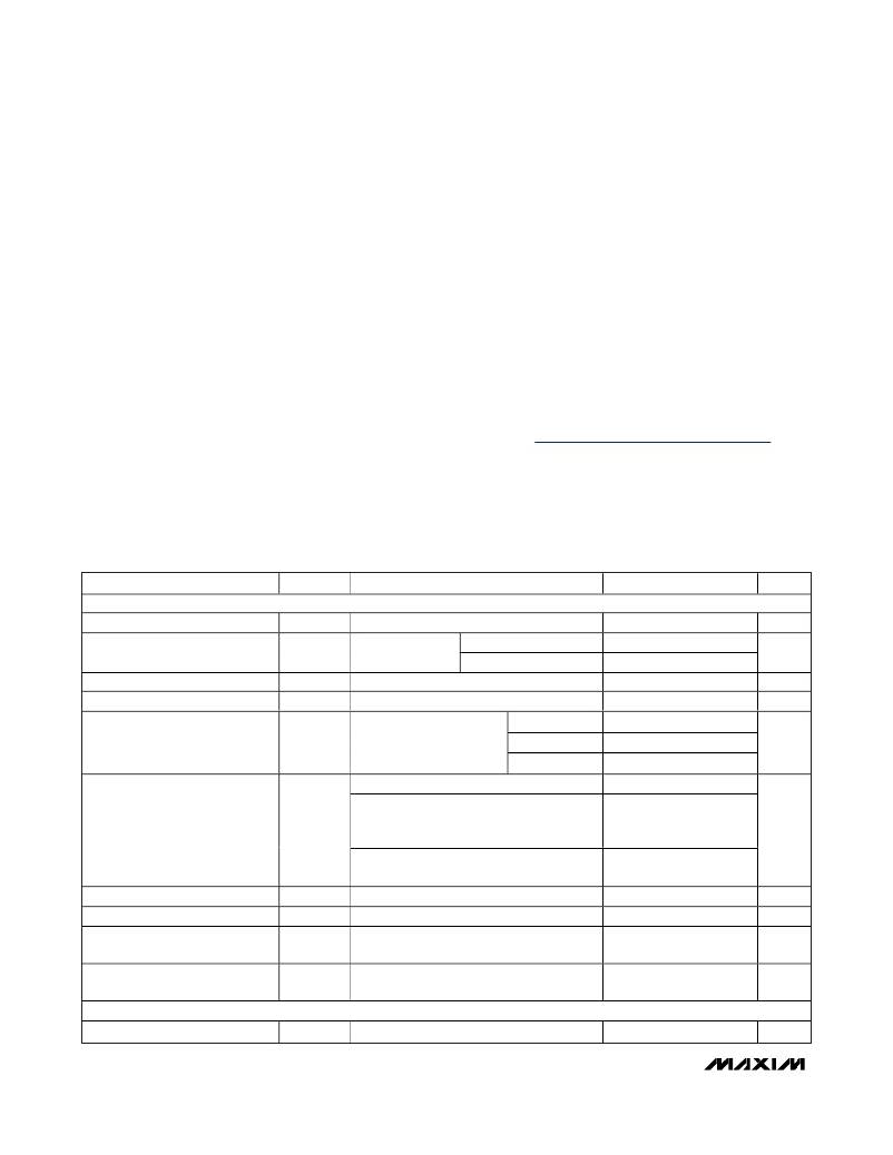
�ELECTRICAL� CHARACTERISTICS�
�(DC,� LX_� unconnected;� V� EP� =� V� GND� =� 0V,� V� BAT� =� 4V,� DLIM[1:2]� =� 00,� EN123� =� EN4� =� low,� V� FB1� =� V� FB2� =� V� FB3� =� 1.1V,� V� FB4� =� 0.6V,�
�PV13� =� PV2� =� SYS,� T� A� =� -40°C� to� +85°C,� capacitors� as� shown� in� Figure� 1,� R� CISET� =� 3k� Ω� ,� unless� otherwise� noted.)� (Note� 3)�
�PARAMETER�
�SYMBOL�
�CONDITIONS�
�MIN�
�TYP�
�MAX�
�UNITS�
�DC� POWER� INPUT�
�DC� Voltage� Range�
�V� DC�
�4.1�
�5.5�
�V�
�SYS� Regulation� Voltage�
�V� SYS_REG�
�V� DC� =� 5.75V�
�MAX8819A/MAX8819C�
�MAX8819B�
�4.3�
�5.1�
�4.35�
�5.3�
�4.4�
�5.5�
�V�
�DC� Undervoltage� Threshold�
�DC� Overvoltage� Threshold�
�V� UVLO_DC�
�V� OVLO_DC�
�V� DC� rising,� 500mV� typical� hysteresis�
�V� DC� rising,� 300mV� typical� hysteresis�
�V� DC� =� 5.75V,� V� SYS� =� 5V�
�DLIM[1:2]� =� 10�
�3.95�
�5.811�
�90�
�4.00�
�5.9�
�95�
�4.05�
�6.000�
�100�
�V�
�V�
�DC� Current� Limit�
�(Note� 4)�
�I� DCLIM�
�for� MAX8819B� or� V� SYS� =�
�4V� for� MAX8819A/�
�DLIM[1:2]� =� 01�
�450�
�475�
�500�
�mA�
�MAX8819C�
�DLIM[1:2]� =� 11� (suspend)�
�DLIM[1:2]� =� 00�
�900�
�1000�
�0.02�
�1100�
�0.035�
�DLIM[1:2]� ≠� 11,� I� SYS� =� 0mA,� I� BAT� =� 0mA,�
�DC� Quiescent� Current�
�I� DCIQ�
�EN123� =� low,� EN4� =� low,� CEN� =� high,�
�V� DC� =� 5.5V�
�1.33�
�mA�
�DLIM[1:2]� ≠� 11,� I� SYS� =� 0mA,� EN123� =� low,�
�EN4� =� low,� CEN� =� low,� V� DC� =� 5.5V�
�0.95�
�DC-to-SYS� Dropout� Resistance�
�R� DS�
�V� DC� =� 4V,� I� SYS� =� 400mA,� DLIM[1:2]� =� 01�
�0.330�
�0.700�
�Ω�
�DC-to-SYS� Soft-Start� Time�
�DC� Thermal-Limit� Temperature�
�DC� Thermal-Limit� Gain�
�t� SS-D-S�
�Die� temperature� where� current� limit� is�
�reduced�
�Amount� of� input� current� reduction� above�
�thermal-limit� temperature�
�1.5�
�100�
�5�
�ms�
�°� C�
�%/� °� C�
�SYSTEM�
�System� Operating� Voltage� Range�
�V� SYS�
�2.6�
�5.5�
�V�
�2�
�_______________________________________________________________________________________�
�相关PDF资料 |
PDF描述 |
|---|---|
| MAX749ESA+T | IC SUPPLY LCD BIAS ADJ 8-SOIC |
| RSA06DRSN-S288 | CONN EDGECARD 12POS .125 EXTEND |
| H3CCS-6406M | IDC CABLE - HKC64S/AE64M/HKC64S |
| UPC3218GV-EVAL | EVAL BOARD FOR UPC3218GV |
| M2MXH-2020K | IDC CABLE - MDM20H/MC20F/X |
相关代理商/技术参数 |
参数描述 |
|---|---|
| MAX8819DETI+ | 功能描述:PMIC 解决方案 PMIC w/Charger & Smart Power Selector RoHS:否 制造商:Texas Instruments 安装风格:SMD/SMT 封装 / 箱体:QFN-24 封装:Reel |
| MAX8819DETI+T | 功能描述:PMIC 解决方案 PMIC w/Charger & Smart Power Selector RoHS:否 制造商:Texas Instruments 安装风格:SMD/SMT 封装 / 箱体:QFN-24 封装:Reel |
| MAX881REUB | 功能描述:PMIC 解决方案 Bias Supply w/Power OK for GaAsFET PA RoHS:否 制造商:Texas Instruments 安装风格:SMD/SMT 封装 / 箱体:QFN-24 封装:Reel |
| MAX881REUB+ | 功能描述:PMIC 解决方案 Bias Supply w/Power OK for GaAsFET PA RoHS:否 制造商:Texas Instruments 安装风格:SMD/SMT 封装 / 箱体:QFN-24 封装:Reel |
| MAX881REUB+T | 功能描述:PMIC 解决方案 Bias Supply w/Power OK for GaAsFET PA RoHS:否 制造商:Texas Instruments 安装风格:SMD/SMT 封装 / 箱体:QFN-24 封装:Reel |
发布紧急采购,3分钟左右您将得到回复。