- 您现在的位置:买卖IC网 > PDF目录1946 > MAX9249GCM/V+ (Maxim Integrated Products)IC SERIALIZER GMSL LVDS 48TQFP PDF资料下载
参数资料
| 型号: | MAX9249GCM/V+ |
| 厂商: | Maxim Integrated Products |
| 文件页数: | 12/36页 |
| 文件大小: | 0K |
| 描述: | IC SERIALIZER GMSL LVDS 48TQFP |
| 产品培训模块: | Lead (SnPb) Finish for COTS Obsolescence Mitigation Program |
| 标准包装: | 250 |
| 功能: | 串行器 |
| 数据速率: | 2.5Gbs |
| 输入类型: | LVDS |
| 输出类型: | 串行 |
| 电源电压: | 3 V ~ 3.6 V |
| 工作温度: | -40°C ~ 105°C |
| 安装类型: | 表面贴装 |
| 封装/外壳: | 48-TQFN 裸露焊盘 |
| 供应商设备封装: | 48-TQFP(7x7) |
| 包装: | 管件 |
第1页第2页第3页第4页第5页第6页第7页第8页第9页第10页第11页当前第12页第13页第14页第15页第16页第17页第18页第19页第20页第21页第22页第23页第24页第25页第26页第27页第28页第29页第30页第31页第32页第33页第34页第35页第36页
2 ______________________________________________________________________________________
MAX9249
Gigabit Multimedia Serial Link
Serializer with LVDS System Interface
Stresses beyond those listed under “Absolute Maximum Ratings” may cause permanent damage to the device. These are stress ratings only, and functional
operation of the device at these or any other conditions beyond those indicated in the operational sections of the specifications is not implied. Exposure to absolute
maximum rating conditions for extended periods may affect device reliability.
AVDD to AGND ....................................................-0.5V to +1.9V
LVDSVDD to AGND..............................................-0.5V to +3.9V
DVDD to GND ......................................................-0.5V to +1.9V
IOVDD to GND .....................................................-0.5V to +3.9V
Any Ground to Any Ground .................................-0.5V to +0.5V
RXIN_ _, RXCLKIN_ to AGND..............................-0.5V to +3.9V
OUT+, OUT- to AGND .........................................-0.5V to +1.9V
LMN_ to AGND (15mA current limit)....................-0.5V to +3.9V
All Other Pins to Any Ground.............. -0.5V to (VIOVDD + 0.5V)
OUT+, OUT- Short Circuit to Ground or Supply .......Continuous
Continuous Power Dissipation (TA = +70NC)
48-Pin TQFP (derate 36.2mW/NC above +70NC)....2898.6mW
ESD Protection
Human Body Model (RD = 1.5kω, CS = 100pF)
(RXIN_ _, RXCLKIN_, OUT+, OUT-) to AGND ................±8kV
All Other Pins to GND......................................................±3kV
IEC 61000-4-2 (RD = 330ω, CS = 150pF)
Contact Discharge
(RXIN_ _, RXCLKIN_) to AGND.......................................±4kV
(OUT+, OUT-) to AGND ................................................±10kV
Air Discharge
(RXIN_ _, RXCLKIN_) to AGND.......................................±8kV
(OUT+, OUT-) to AGND ................................................±12kV
ISO 10605 (RD = 2kω, CS = 330pF)
Contact Discharge
(RXIN_ _, RXCLKIN_) to AGND.......................................±6kV
(OUT+, OUT-) to AGND ................................................±10kV
Air Discharge
(RXIN_ _, RXCLKIN_) to AGND.....................................±20kV
(OUT+, OUT-) to AGND ................................................±30kV
Operating Temperature Range........................ -40NC to +105NC
Junction Temperature .....................................................+150NC
Storage Temperature Range............................ -65NC to +150NC
Lead Temperature (soldering, 10s) ................................+300NC
Soldering Temperature (reflow) ......................................+260NC
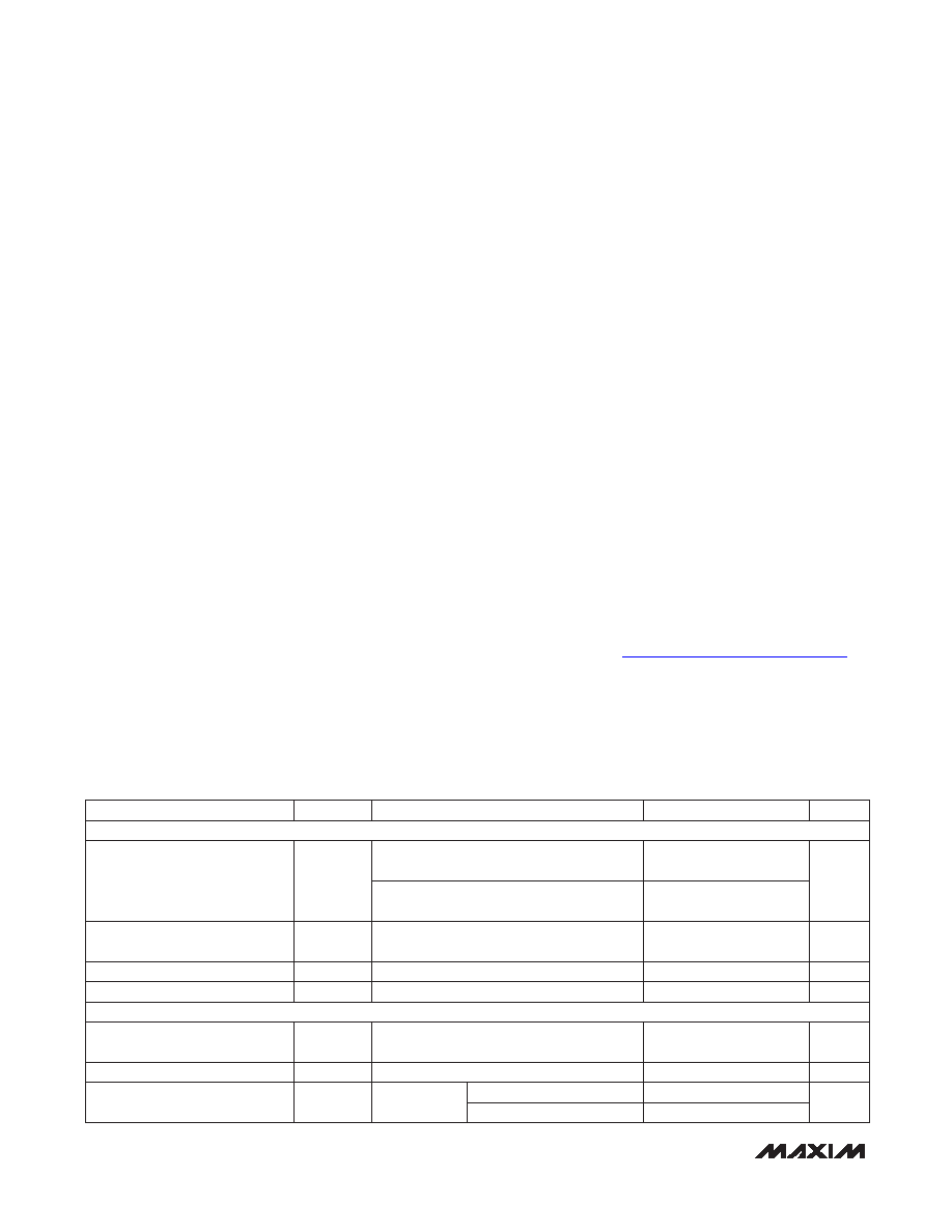
DC ELECTRICAL CHARACTERISTICS
(VDVDD = VAVDD = 1.7V to 1.9V, VLVDSVDD = 3.0V to 3.6V, VIOVDD = 1.7V to 3.6V, RL = 100I ±1% (differential), TA = -40NC to
+105NC, unless otherwise noted. Differential input voltage |VID| = 0.1V to 1.2V, input common-mode voltage VCM = |VID/2| to 2.4V
- |VID/2|. Typical values are at VDVDD = VAVDD = VIOVDD = 1.8V, VLVDSVDD = 3.3V, TA = +25NC.)
ABSOLUTE MAXIMUM RATINGS
PACKAGE THERMAL CHARACTERISTICS (Note 1)
48 TQFP-EP
Junction-to-Ambient Thermal Resistance (θJA).......27.6NC/W
Junction-to-Case Thermal Resistance (θJC).................2NC/W
Note 1: Package thermal resistances were obtained using the method described in JEDEC specification JESD51-7, using a four-
layer board. For detailed information on package thermal considerations, refer to www.maxim-ic.com/thermal-tutorial.
PARAMETER
SYMBOL
CONDITIONS
MIN
TYP
MAX
UNITS
SINGLE-ENDED INPUTS (PWDN, SSEN, BWS, DRS, MS, CDS, AUTOS, SD/CNTL0, SCK, WS, CNTL_)
High-Level Input Voltage
VIH1
PWDN, SSEN, BWS, DRS, MS, CDS, AUTOS
0.65 x
VIOVDD
V
SD/CNTL0, SCK, WS, CNTL_
0.7 x
VIOVDD
Low-Level Input Voltage
VIL1
0.35 x
VIOVDD
V
Input Current
IIN1
VIN = 0 to VIOVDD
-10
+10
F
A
Input Clamp Voltage
VCL
ICL = -18mA
-1.5
V
SINGLE-ENDED OUTPUT (INT)
High-Level Output Voltage
VOH1
IOH = -2mA
VIOVDD -
0.2
V
Low-Level Output Voltage
VOL1
IOL = 2mA
0.2
V
Output Short-Circuit Current
IOS
VO = 0V
VIOVDD = 3.0V to 3.6V
16
35
64
mA
VIOVDD = 1.7V to 1.9V
3
12
21
相关PDF资料 |
PDF描述 |
|---|---|
| MAX9257AGTL/V+ | IC SERDE PROG UART/I2C 40TQFN |
| MAX9257GTL+T | IC SER/DESER PROG 40-TQFN |
| MAX9260GCB/V+ | IC DESERIALIZER GMSL 64TQFP |
| MAX9271GTJ/V+ | IC SERIALIZER 16BIT GMSL 32TQFN |
| MAX9272GTM/V+ | IC DSERIALIZER 28BIT GMSL 48TQFN |
相关代理商/技术参数 |
参数描述 |
|---|---|
| MAX924C/D | 功能描述:校验器 IC RoHS:否 制造商:STMicroelectronics 产品: 比较器类型: 通道数量: 输出类型:Push-Pull 电源电压-最大:5.5 V 电源电压-最小:1.1 V 补偿电压(最大值):6 mV 电源电流(最大值):1350 nA 响应时间: 最大工作温度:+ 125 C 安装风格:SMD/SMT 封装 / 箱体:SC-70-5 封装:Reel |
| MAX924CPE | 功能描述:校验器 IC RoHS:否 制造商:STMicroelectronics 产品: 比较器类型: 通道数量: 输出类型:Push-Pull 电源电压-最大:5.5 V 电源电压-最小:1.1 V 补偿电压(最大值):6 mV 电源电流(最大值):1350 nA 响应时间: 最大工作温度:+ 125 C 安装风格:SMD/SMT 封装 / 箱体:SC-70-5 封装:Reel |
| MAX924CPE+ | 功能描述:校验器 IC Quad Comparator w/1% Precision Ref RoHS:否 制造商:STMicroelectronics 产品: 比较器类型: 通道数量: 输出类型:Push-Pull 电源电压-最大:5.5 V 电源电压-最小:1.1 V 补偿电压(最大值):6 mV 电源电流(最大值):1350 nA 响应时间: 最大工作温度:+ 125 C 安装风格:SMD/SMT 封装 / 箱体:SC-70-5 封装:Reel |
| MAX924CSE | 功能描述:校验器 IC Quad Comparator w/1% Precision Ref RoHS:否 制造商:STMicroelectronics 产品: 比较器类型: 通道数量: 输出类型:Push-Pull 电源电压-最大:5.5 V 电源电压-最小:1.1 V 补偿电压(最大值):6 mV 电源电流(最大值):1350 nA 响应时间: 最大工作温度:+ 125 C 安装风格:SMD/SMT 封装 / 箱体:SC-70-5 封装:Reel |
| MAX924CSE+ | 功能描述:校验器 IC Quad Comparator w/1% Precision Ref RoHS:否 制造商:STMicroelectronics 产品: 比较器类型: 通道数量: 输出类型:Push-Pull 电源电压-最大:5.5 V 电源电压-最小:1.1 V 补偿电压(最大值):6 mV 电源电流(最大值):1350 nA 响应时间: 最大工作温度:+ 125 C 安装风格:SMD/SMT 封装 / 箱体:SC-70-5 封装:Reel |
发布紧急采购,3分钟左右您将得到回复。