- 您现在的位置:买卖IC网 > PDF目录11144 > MAX9670CTL+T (Maxim Integrated Products)IC AUDIO/VIDEO SWIT DUAL 40TQFN PDF资料下载
参数资料
| 型号: | MAX9670CTL+T |
| 厂商: | Maxim Integrated Products |
| 文件页数: | 12/44页 |
| 文件大小: | 0K |
| 描述: | IC AUDIO/VIDEO SWIT DUAL 40TQFN |
| 产品培训模块: | Lead (SnPb) Finish for COTS Obsolescence Mitigation Program |
| 标准包装: | 2,500 |
| 功能: | 音频/视频切换 |
| 电路: | 2 x SCART |
| 电压电源: | 单电源 |
| 电压 - 电源,单路/双路(±): | 3.3 V ~ 12 V |
| 工作温度: | 0°C ~ 70°C |
| 安装类型: | 表面贴装 |
| 封装/外壳: | 40-WFQFN 裸露焊盘 |
| 供应商设备封装: | 40-TQFN-EP(6x6) |
| 包装: | 带卷 (TR) |
| 配用: | MAX9670EVKIT+-ND - EVALUATION KIT FOR MAX9670 |
第1页第2页第3页第4页第5页第6页第7页第8页第9页第10页第11页当前第12页第13页第14页第15页第16页第17页第18页第19页第20页第21页第22页第23页第24页第25页第26页第27页第28页第29页第30页第31页第32页第33页第34页第35页第36页第37页第38页第39页第40页第41页第42页第43页第44页
MAX9670/MAX9671
Low-Power Audio/Video Switch with Audio
Volume Control for Dual SCART Connectors
2
_______________________________________________________________________________________
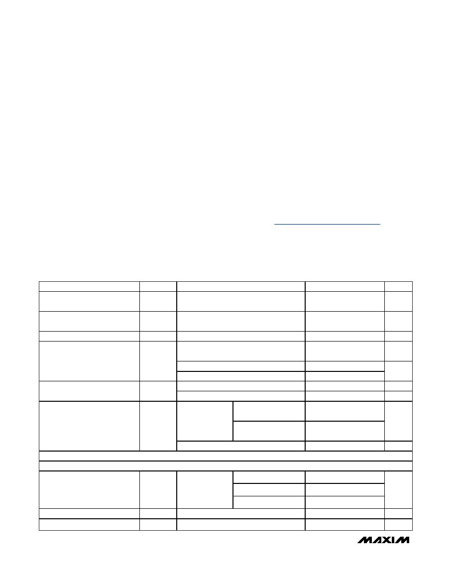
ABSOLUTE MAXIMUM RATINGS
ELECTRICAL CHARACTERISTICS
(V12 = 12V, VVID = VAUD = 3.3V, VGNDVID = VEP = 0V, no load, TA = 0°C to +70°C, unless otherwise noted. Typical values are at
TA = +25°C.) (Note 2)
Stresses beyond those listed under “Absolute Maximum Ratings” may cause permanent damage to the device. These are stress ratings only, and functional
operation of the device at these or any other conditions beyond those indicated in the operational sections of the specifications is not implied. Exposure to
absolute maximum rating conditions for extended periods may affect device reliability.
VVID to GNDVID........................................................-0.3V to +4V
V12 to EP.................................................................-0.3V to +14V
VAUD to EP ...............................................................-0.3V to +4V
EP to GNDVID .......................................................-0.1V to +0.1V
All Video Inputs, VCRIN_FS to GNDVID...................-0.3V to +4V
All Audio Inputs to EP .......................................-1V to (VEP + 1V)
SDA, SCL, DEV_ADDR, INT to GNDVID ..................-0.3V to +4V
TV_SS, VCR_SS to EP .................................-0.3V to (V12 + 0.3V)
Current
All Video/Audio Inputs ...................................................±20mA
C1P, C1N, CPVSS .........................................................±50mA
Output Short-Circuit Current Duration
Video and Fast-Switching Outputs to VVID,
GNDVID.................................................................Continuous
Audio Outputs to VAUD, EP .....................................Continuous
TV_SS, VCR_SS to V12, EP......................................Continuous
Continuous Power Dissipation (TA = +70°C)
40-Pin TQFN-EP (derate 26.3mW/°C above +70°C) ...2105.3mW
44-Pin TQFN-EP (derate 26.3mW/°C above +70°C)...2222.2mW
Junction-to-Case Thermal Resistance (
θJC) (Note 1)
40/44-pin TQFN-EP .........................................................1°C/W
Junction-to-Ambient Thermal Resistance (
θJA) (Note 1)
40/44-pin TQFN-EP .......................................................27°C/W
Operating Temperature Range...............................0°C to +70°C
Junction Temperature ......................................................+150°C
Storage Temperature Range .............................-65°C to +150°C
Lead Temperature (soldering, 10s) .................................+300°C
Soldering Temperature (reflow) .......................................+260°C
PARAMETER
SYMBOL
CONDITIONS
MIN
TYP
MAX
UNITS
Video Supply Voltage Range
VVID
Inferred from video PSRR test at 3V and
3.6V
3
3.3
3.6
V
Audio Supply Voltage Range
VAUD
Inferred from audio PSRR test at 3V and
3.6V
3
3.3
3.6
V
V12 Supply Voltage Range
V12
Inferred from slow-switching levels
11.4
12
12.6
V
Normal operation; all video output
amplifiers are enabled and muted (Note 3)
16
30
mA
Standby mode, slow switch inputs low
1500
VVID Quiescent Supply Current
IVID_Q
Shutdown
35
A
Normal operation (Note 3)
3.2
6
mA
VAUD Quiescent Supply Current
IAUD_Q
Shutdown
35
A
Slow-switching output
set to low-level
0.3
100
Normal operation
(Note 3)
Slow-switching output
set to medium-level
475
A
V12 Quiescent Supply Current
I12_Q
Shutdown, TA = +25°C
10
A
VIDEO CHARACTERISTICS
DC-COUPLED INPUT
VVID = 3V
1.15
VVID = 3.135V
1.15
Input Voltage Range
VIN
RL = 75
to
GNDVID or 150
to VVID/2; inferred
from gain test
VVID = 3.3V
1.3
VP-P
Input Current
IIN
VIN = 0.3V, TA = +25°C
1
2
A
Input Resistance
RIN
300
k
Note 1: Package thermal resistance were obtained using the method described in JEDEC specification JESD51-7, using a four-layer
board. For detailed information on package thermal considerations, refer to www.maxim-ic.com/thermal-tutorial.
相关PDF资料 |
PDF描述 |
|---|---|
| VE-B60-IX-F1 | CONVERTER MOD DC/DC 5V 75W |
| MAX4751EGE+T | IC SWITCH QUAD SPST 16QFN |
| VE-B60-IW-F4 | CONVERTER MOD DC/DC 5V 100W |
| VE-B60-IW-F3 | CONVERTER MOD DC/DC 5V 100W |
| VE-B60-IW-F1 | CONVERTER MOD DC/DC 5V 100W |
相关代理商/技术参数 |
参数描述 |
|---|---|
| MAX9670EVKIT+ | 功能描述:交换机 IC 开发工具 Low-Power A/V Switch w/Audio Volume Cntrl RoHS:否 制造商:Maxim Integrated 产品:Evaluation Kits 类型:USB Power Switches 工具用于评估:MAX4984E 工作电源电压:2.8 V to 5.5 V |
| MAX9671CTH+ | 功能描述:视频开关 IC Low-Power A/V Switch w/Audio Volume Cntrl RoHS:否 制造商:Texas Instruments 开关数量:4 开启电阻(最大值):12 Ohms 传播延迟时间: 开启时间(最大值): 关闭时间(最大值): 最大工作温度:+ 85 C 最小工作温度:- 40 C 封装 / 箱体:WQFN-42 封装:Reel |
| MAX9671CTH+T | 功能描述:视频开关 IC Low-Power A/V Switch w/Audio Volume Cntrl RoHS:否 制造商:Texas Instruments 开关数量:4 开启电阻(最大值):12 Ohms 传播延迟时间: 开启时间(最大值): 关闭时间(最大值): 最大工作温度:+ 85 C 最小工作温度:- 40 C 封装 / 箱体:WQFN-42 封装:Reel |
| MAX9671EVKIT+ | 功能描述:交换机 IC 开发工具 Low-Power A/V Switch w/Audio Volume Cntrl RoHS:否 制造商:Maxim Integrated 产品:Evaluation Kits 类型:USB Power Switches 工具用于评估:MAX4984E 工作电源电压:2.8 V to 5.5 V |
| MAX9672ETI+ | 功能描述:LCD Gamma缓冲器 10-Bit Prog Gamma Reference System RoHS:否 制造商:Maxim Integrated 输入补偿电压: 转换速度: 电源电压-最大:20 V 电源电压-最小:9 V 电源电流: 最大功率耗散: 最大工作温度:+ 85 C 安装风格:SMD/SMT 封装 / 箱体:TQFN-38 封装:Tube |
发布紧急采购,3分钟左右您将得到回复。