- 您现在的位置:买卖IC网 > PDF目录11144 > MAX9670CTL+T (Maxim Integrated Products)IC AUDIO/VIDEO SWIT DUAL 40TQFN PDF资料下载
参数资料
| 型号: | MAX9670CTL+T |
| 厂商: | Maxim Integrated Products |
| 文件页数: | 20/44页 |
| 文件大小: | 0K |
| 描述: | IC AUDIO/VIDEO SWIT DUAL 40TQFN |
| 产品培训模块: | Lead (SnPb) Finish for COTS Obsolescence Mitigation Program |
| 标准包装: | 2,500 |
| 功能: | 音频/视频切换 |
| 电路: | 2 x SCART |
| 电压电源: | 单电源 |
| 电压 - 电源,单路/双路(±): | 3.3 V ~ 12 V |
| 工作温度: | 0°C ~ 70°C |
| 安装类型: | 表面贴装 |
| 封装/外壳: | 40-WFQFN 裸露焊盘 |
| 供应商设备封装: | 40-TQFN-EP(6x6) |
| 包装: | 带卷 (TR) |
| 配用: | MAX9670EVKIT+-ND - EVALUATION KIT FOR MAX9670 |
第1页第2页第3页第4页第5页第6页第7页第8页第9页第10页第11页第12页第13页第14页第15页第16页第17页第18页第19页当前第20页第21页第22页第23页第24页第25页第26页第27页第28页第29页第30页第31页第32页第33页第34页第35页第36页第37页第38页第39页第40页第41页第42页第43页第44页
MAX9670/MAX9671
Low-Power Audio/Video Switch with Audio
Volume Control for Dual SCART Connectors
______________________________________________________________________________________
27
Similarly, when YPbPr signals are desired, ENC_R/C_IN,
ENC_G_IN, and ENC_B_IN of the MAX9670/MAX9671
should be set to high-impedance mode by setting bit 4 in
register 08h to high if those video inputs are AC-coupled.
The high-impedance mode has higher priority whether
ENC_R/C_IN is in sync-tip clamp or bias circuit mode
(set by bit 3 in register 08h). If ENC_R/C_IN, ENC_G_IN,
and ENC_B_IN are DC-coupled, the inputs should be left
in sync-tip clamp mode. The RGB outputs of the
MAX9670/MAX9671 should be muted or shut down.
In either case, the inactive device should not distort the
video signals generated by the DACs.
Power-Supply Bypassing
The MAX9670/MAX9671 feature single 3.3V and 12V
supply operation and require no negative supply. The
12V supply V12 is for the SCART switching function. For
V12, place a 0.1F bypass capacitor as close as possi-
ble. Connect all VAUD pins together to 3.3V and bypass
with a 10F electrolytic capacitor in parallel with a
0.1F ceramic capacitor to audio ground. Bypass each
VVID to video ground with a 0.1F ceramic capacitor.
Using a Digital Supply
The MAX9670/MAX9671 are designed to operate from
noisy digital supplies. The high PSRR (49dB at 100kHz)
allows the MAX9670/MAX9671 to reject the noise from
the digital power supplies (see the
Typical Operating
Characteristics). If the digital power supply is very noisy
and stripes appear on the television screen, increase
the supply bypass capacitance. An additional, smaller
capacitor in parallel with the main bypass capacitor
can reduce digital supply noise because the smaller
capacitor has lower equivalent series resistance (ESR)
and equivalent series inductance (ESL).
Layout and Grounding
For optimal performance, use controlled-impedance
traces for video signal paths and place input termina-
tion resistors and output back-termination resistors
close to the MAX9670/MAX9671. Avoid routing video
traces parallel to high-speed data lines.
The MAX9670/MAX9671 provide separate ground con-
nections for video and audio supplies. For best perfor-
mance, use separate ground planes for each of the
ground returns and connect all ground planes together
at a single point. See the MAX9670/MAX9671 evalua-
tion kit for a proven circuit board layout example.
If the MAX9670/MAX9671 are mounted using flow sol-
dering or wave soldering, the ground via(s) for the EP
pad should have a finished hole size of at least 14mils
to insure adequate wicking of soldering onto the
exposed pad. If the MAX9670/MAX9671 are mounted
using solder mask technique, the via requirement does
not apply. In either case, a good connection between
the exposed pad and ground is required to minimize
noise from coupling onto the outputs.
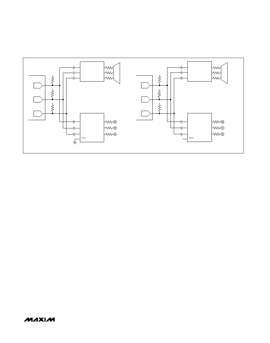
Figure 19. Triple DAC is connected to both a MAX9670/MAX9671 and a MAX9653/MAX9654 high-definition video-filter amplifier. (A)
The MAX9670/MAX9671 are transmitting standard-definition RGB signals while the MAX9653/MAX9654 are in shutdown mode. (B)
The MAX9670/MAX9671 are not transmitting RGB signals, but the MAX9653/MAX9654 are transmitting high-definition YPbPr signals.
DAC
SET-TOP BOX
CHIP
ENC_R/C_IN
ENC_G_IN
ENC_B_IN
75
75
75
TV_R/C_OUT
TV_G_OUT
TV_B_OUT
MAX9653
MAX9654
SCART
CONNECTOR
OFF
YPbPr OUTPUTS
(A)
75
75
75
YOUT
PBOUT
PROUT
YIN
PBIN
PRIN
SHDN
DAC
3.3V
DAC
SET-TOP BOX
CHIP
ENC_R/C_IN
ENC_G_IN
ENC_B_IN
MAX9670/MAX9671
75
75
75
0.1
F
0.1
F
0.1
F
0.1
F
0.1
F
0.1
F
0.1
F
0.1
F
0.1
F
TV_R/C_OUT
TV_G_OUT
TV_B_OUT
MAX9653
MAX9654
3.3V
SCART
CONNECTOR
INPUTS SET TO HIGH IMPEDANCE
INPUTS SET TO SYNC-TIP CLAMP
ON
YPbPr OUTPUTS
(B)
75
75
75
YOUT
PBOUT
PROUT
YIN
PBIN
PRIN
SHDN
相关PDF资料 |
PDF描述 |
|---|---|
| VE-B60-IX-F1 | CONVERTER MOD DC/DC 5V 75W |
| MAX4751EGE+T | IC SWITCH QUAD SPST 16QFN |
| VE-B60-IW-F4 | CONVERTER MOD DC/DC 5V 100W |
| VE-B60-IW-F3 | CONVERTER MOD DC/DC 5V 100W |
| VE-B60-IW-F1 | CONVERTER MOD DC/DC 5V 100W |
相关代理商/技术参数 |
参数描述 |
|---|---|
| MAX9670EVKIT+ | 功能描述:交换机 IC 开发工具 Low-Power A/V Switch w/Audio Volume Cntrl RoHS:否 制造商:Maxim Integrated 产品:Evaluation Kits 类型:USB Power Switches 工具用于评估:MAX4984E 工作电源电压:2.8 V to 5.5 V |
| MAX9671CTH+ | 功能描述:视频开关 IC Low-Power A/V Switch w/Audio Volume Cntrl RoHS:否 制造商:Texas Instruments 开关数量:4 开启电阻(最大值):12 Ohms 传播延迟时间: 开启时间(最大值): 关闭时间(最大值): 最大工作温度:+ 85 C 最小工作温度:- 40 C 封装 / 箱体:WQFN-42 封装:Reel |
| MAX9671CTH+T | 功能描述:视频开关 IC Low-Power A/V Switch w/Audio Volume Cntrl RoHS:否 制造商:Texas Instruments 开关数量:4 开启电阻(最大值):12 Ohms 传播延迟时间: 开启时间(最大值): 关闭时间(最大值): 最大工作温度:+ 85 C 最小工作温度:- 40 C 封装 / 箱体:WQFN-42 封装:Reel |
| MAX9671EVKIT+ | 功能描述:交换机 IC 开发工具 Low-Power A/V Switch w/Audio Volume Cntrl RoHS:否 制造商:Maxim Integrated 产品:Evaluation Kits 类型:USB Power Switches 工具用于评估:MAX4984E 工作电源电压:2.8 V to 5.5 V |
| MAX9672ETI+ | 功能描述:LCD Gamma缓冲器 10-Bit Prog Gamma Reference System RoHS:否 制造商:Maxim Integrated 输入补偿电压: 转换速度: 电源电压-最大:20 V 电源电压-最小:9 V 电源电流: 最大功率耗散: 最大工作温度:+ 85 C 安装风格:SMD/SMT 封装 / 箱体:TQFN-38 封装:Tube |
发布紧急采购,3分钟左右您将得到回复。