- 您现在的位置:买卖IC网 > PDF目录11144 > MAX9670CTL+T (Maxim Integrated Products)IC AUDIO/VIDEO SWIT DUAL 40TQFN PDF资料下载
参数资料
| 型号: | MAX9670CTL+T |
| 厂商: | Maxim Integrated Products |
| 文件页数: | 7/44页 |
| 文件大小: | 0K |
| 描述: | IC AUDIO/VIDEO SWIT DUAL 40TQFN |
| 产品培训模块: | Lead (SnPb) Finish for COTS Obsolescence Mitigation Program |
| 标准包装: | 2,500 |
| 功能: | 音频/视频切换 |
| 电路: | 2 x SCART |
| 电压电源: | 单电源 |
| 电压 - 电源,单路/双路(±): | 3.3 V ~ 12 V |
| 工作温度: | 0°C ~ 70°C |
| 安装类型: | 表面贴装 |
| 封装/外壳: | 40-WFQFN 裸露焊盘 |
| 供应商设备封装: | 40-TQFN-EP(6x6) |
| 包装: | 带卷 (TR) |
| 配用: | MAX9670EVKIT+-ND - EVALUATION KIT FOR MAX9670 |
第1页第2页第3页第4页第5页第6页当前第7页第8页第9页第10页第11页第12页第13页第14页第15页第16页第17页第18页第19页第20页第21页第22页第23页第24页第25页第26页第27页第28页第29页第30页第31页第32页第33页第34页第35页第36页第37页第38页第39页第40页第41页第42页第43页第44页
MAX9670/MAX9671
Low-Power Audio/Video Switch with Audio
Volume Control for Dual SCART Connectors
______________________________________________________________________________________
15
Clickless Switching
The TV audio channel incorporates a zero-crossing
detect (ZCD) circuit that minimizes click noise due to
abrupt signal level changes that occur when switching
between audio signals at an arbitrary moment.
To implement the zero-crossing function when switch-
ing audio signals, set the ZCD bit high (Audio Control
register 00h, bit 6). Then set the mute bit high (Audio
Control register 00h, bit 0). Next, wait for a sufficient
period of time for the audio signal to cross zero. This
period is a function of the audio signal path’s low-fre-
quency 3dB corner (fL3dB). Thus, if fL3dB = 20Hz, the
time period to wait for a zero-crossing detect is 1/20Hz
or 50ms.
After the wait period, select a new audio source for the
TV audio channel by writing to bits 1 and 0 of TV Audio
Control register (01h). Finally, clear mute (Audio Control
register, 00h, bit 0), but leave ZCD (Audio Control reg-
ister 00h, bit 6) high. The MAX9670/MAX9671 switches
the signal out of mute at the next zero crossing. See
Tables 12 and 13.
Audio Outputs
The MAX9670/MAX9671 audio output amplifiers feature
Maxim’s DirectDrive architecture, thereby eliminating
the need for output-coupling capacitors required by
conventional single-supply audio line drivers. An inter-
nal charge pump inverts the positive supply (VAUD),
creating a negative supply (CPVSS). The audio output
amplifiers operate from these bipolar supplies with their
outputs biased about audio ground (Figure 2). The ben-
efit of this audio ground bias is that the amplifier out-
puts do not have a DC component. The DC-blocking
capacitors required with conventional audio line drivers
are unnecessary, conserving board space, reducing
system cost, and improving frequency response.
Conventional single-supply audio line drivers have their
outputs biased about a nominal DC voltage (typically
half the supply) for maximum dynamic range. Large
coupling capacitors are needed to block this DC bias.
Clicks and pops are created when the coupling capaci-
tors are charged during power-up and discharged dur-
ing power-down.
The MAX9670/MAX9671 features a low-noise charge
pump that requires only two small ceramic capacitors.
The 580kHz switching frequency is well beyond the
audio range and does not interfere with audio signals.
The switch drivers feature a controlled switching speed
that minimizes noise generated by turn-on and turn-off
transients.
The SCART standard specifies 2VRMS as the full-scale
for audio signals. As the audio circuits process
0.5VRMS full-scale audio signals internal to the
MAX9670/MAX9671, the gain-of-4 output amplifiers
restore the audio signals to a full-scale of 2VRMS.
To select which audio input source is routed to the TV
SCART connector, write to bits 1 and 0 of the TV Audio
Control register (01h). To select which audio input
source is routed to the VCR SCART connector, write to
bits 3 and 2 of the TV Audio Control register (01h). The
power-on default is for the TV and VCR audio outputs to
be muted (the inputs of the output amplifiers are con-
nected to audio ground). See Tables 10 and 13.
Volume Control
Volume control is programmable from -62dB to 0dB in
2dB steps through I2C interface. The block consists of
a resistive ladder network to generate 31 2dB volume
control steps, a unity gain buffer to isolate the input
from the resistive ladder, switches (MPLx and MNLx)
that select 1 of 32 nodes on the resistive ladder, and
logic to decode the the I2C volume control value. See
Table 12.
+VDD
-VDD
GND
VOUT
CONVENTIONAL DRIVER-BIASING SCHEME
DirectDrive BIASING SCHEME
VDD/2
VDD
GND
2VDD
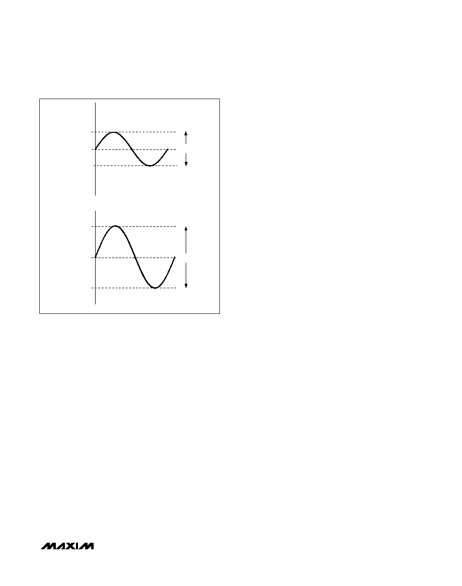
Figure 2. Conventional Driver Output Waveform vs. MAX9670/
MAX9671 Output Waveform.
相关PDF资料 |
PDF描述 |
|---|---|
| VE-B60-IX-F1 | CONVERTER MOD DC/DC 5V 75W |
| MAX4751EGE+T | IC SWITCH QUAD SPST 16QFN |
| VE-B60-IW-F4 | CONVERTER MOD DC/DC 5V 100W |
| VE-B60-IW-F3 | CONVERTER MOD DC/DC 5V 100W |
| VE-B60-IW-F1 | CONVERTER MOD DC/DC 5V 100W |
相关代理商/技术参数 |
参数描述 |
|---|---|
| MAX9670EVKIT+ | 功能描述:交换机 IC 开发工具 Low-Power A/V Switch w/Audio Volume Cntrl RoHS:否 制造商:Maxim Integrated 产品:Evaluation Kits 类型:USB Power Switches 工具用于评估:MAX4984E 工作电源电压:2.8 V to 5.5 V |
| MAX9671CTH+ | 功能描述:视频开关 IC Low-Power A/V Switch w/Audio Volume Cntrl RoHS:否 制造商:Texas Instruments 开关数量:4 开启电阻(最大值):12 Ohms 传播延迟时间: 开启时间(最大值): 关闭时间(最大值): 最大工作温度:+ 85 C 最小工作温度:- 40 C 封装 / 箱体:WQFN-42 封装:Reel |
| MAX9671CTH+T | 功能描述:视频开关 IC Low-Power A/V Switch w/Audio Volume Cntrl RoHS:否 制造商:Texas Instruments 开关数量:4 开启电阻(最大值):12 Ohms 传播延迟时间: 开启时间(最大值): 关闭时间(最大值): 最大工作温度:+ 85 C 最小工作温度:- 40 C 封装 / 箱体:WQFN-42 封装:Reel |
| MAX9671EVKIT+ | 功能描述:交换机 IC 开发工具 Low-Power A/V Switch w/Audio Volume Cntrl RoHS:否 制造商:Maxim Integrated 产品:Evaluation Kits 类型:USB Power Switches 工具用于评估:MAX4984E 工作电源电压:2.8 V to 5.5 V |
| MAX9672ETI+ | 功能描述:LCD Gamma缓冲器 10-Bit Prog Gamma Reference System RoHS:否 制造商:Maxim Integrated 输入补偿电压: 转换速度: 电源电压-最大:20 V 电源电压-最小:9 V 电源电流: 最大功率耗散: 最大工作温度:+ 85 C 安装风格:SMD/SMT 封装 / 箱体:TQFN-38 封装:Tube |
发布紧急采购,3分钟左右您将得到回复。