- 您现在的位置:买卖IC网 > PDF目录180540 > MAX9961BLCCQ-TD (MAXIM INTEGRATED PRODUCTS INC) Dual, Low-Power, 500Mbps ATE Drivers/Comparators with 2mA Load PDF资料下载
参数资料
| 型号: | MAX9961BLCCQ-TD |
| 厂商: | MAXIM INTEGRATED PRODUCTS INC |
| 元件分类: | 比较器 |
| 英文描述: | Dual, Low-Power, 500Mbps ATE Drivers/Comparators with 2mA Load |
| 中文描述: | DUAL COMPARATOR, 100000 uV OFFSET-MAX, 2.2 ns RESPONSE TIME, PQFP100 |
| 封装: | 14 X 14 MM, 1 MM HEIGHT, 0.50 MM PITCH, TQFP-100 |
| 文件页数: | 14/30页 |
| 文件大小: | 740K |
| 代理商: | MAX9961BLCCQ-TD |
第1页第2页第3页第4页第5页第6页第7页第8页第9页第10页第11页第12页第13页当前第14页第15页第16页第17页第18页第19页第20页第21页第22页第23页第24页第25页第26页第27页第28页第29页第30页
MAX9961/MAX9962
Dual, Low-Power, 500Mbps
ATE Drivers/Comparators with 2mA Load
______________________________________________________________________________________
21
Output Driver
The driver input is a high-speed multiplexer that selects
one of three voltage inputs: DHV_, DLV_, or DTV_. This
switching is controlled by high-speed inputs DATA_
and RCV_, and mode-control bit TMSEL (Table 1). A
slew-rate circuit controls the slew rate of the buffer
input. Select to one of four possible slew rates accord-
ing to Table 2. The speed of the internal multiplexer
sets the 100% driver slew rate (see the Driver Large-
Signal Response graph in the Typical Operating
Characteristics).
DUT_ can be toggled at high speed between the buffer
output and high-impedance mode, or it can be placed
into low-leakage mode (Figure 2, Table 1). In high-
impedance mode the clamps are connected. High-
speed input RCV_ and mode control bits TMSEL and
LLEAK control the switching. In high-impedance mode,
the bias current at DUT_ is less than 1.5A over the 0 to
3V range, while the node maintains its ability to track
high-speed signals. In low-leakage mode, the bias cur-
rent at DUT_ is further reduced to less than 15nA, and
signal tracking slows. See the Low-Leakage Mode sec-
tion for more details.
The nominal driver output resistance is 50
. Contact
the factory for different resistance values within the 45
to 51
range.
Clamps
Configure the voltage clamps (high and low) to limit the
voltage at DUT_ and to suppress reflections when the
channel is configured as a high-impedance receiver.
The clamps behave as diodes connected to the outputs
of high-current buffers. Internal circuitry compensates
for the diode drop at 1mA clamp current. Set the clamp
voltages using the external connections CPHV_ and
CPLV_. The clamps are enabled only when the driver is
in the high-impedance mode (Figure 2). For transient
suppression, set the clamp voltages to approximately
the minimum and maximum expected DUT_ voltage
range. The optimal clamp voltages are application spe-
cific and must be empirically determined. If clamping is
not desired, set the clamp voltages at least 0.7V out-
side the expected DUT_ voltage range; overvoltage
protection remains active without loading DUT_.
Comparators
The MAX9961/MAX9962 provide two independent high-
speed comparators for each channel. Each comparator
has one input connected internally to DUT_ and the
other input connected to either CHV_ or CLV_ (see the
Functional Diagram). Comparator outputs are a logical
result of the input conditions, as indicated in Table 3.
The comparator differential outputs are open collector.
This configuration switches an 8mA current source
between the two outputs, and is available with and with-
out internal termination resistors connected to VCCO_
(Figure 3). For external termination, leave VCCO_ uncon-
nected and add the required external resistors. These
resistors are typically 50
to the pullup voltage at the
receiving end of the output trace. Alternate configura-
tions to terminate different path impedances can be
used provided that the Absolute Maximum Ratings are
not exceeded. Note that the resistor value also sets the
voltage swing. For internal termination, connect VCCO_
to the desired VOH voltage. The output provides a nomi-
nal 400mVP-P swing and 50
source termination.
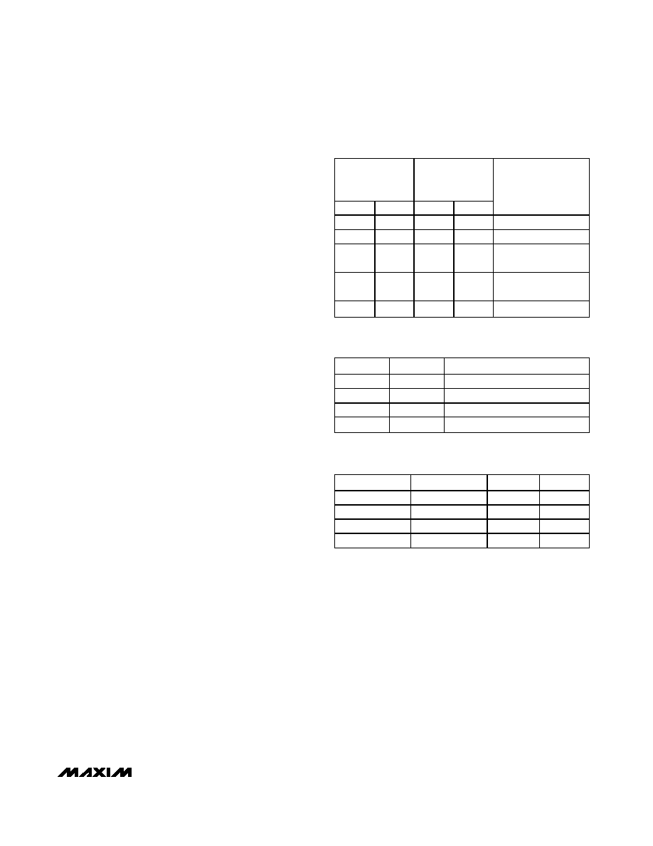
Table 1. Driver Logic
EXTERNAL
CONNECTIONS
INTERNAL
CONTROL
REGISTER
DATA_
RCV_
TMSEL
LLEAK
DRIVER OUTPUT
1
0
X
0
Drive to DHV_
0
X
0
Drive to DLV_
X1
1
0
Drive to DTV_
(term mode)
X1
0
High-impedance
mode (high-z)
X
1
Low-leakage mode
Table 2. Slew Rate Logic
SC1
SC0
DRIVER SLEW RATE (%)
0
100
01
75
10
50
11
25
Table 3. Comparator Logic
DUT_ > CHV_
DUT_ > CLV_
CH_
CL_
00
0
01
0
1
10
1
0
11
1
相关PDF资料 |
PDF描述 |
|---|---|
| MAX9967BRCCQ-TD | Dual, Low-Power, 500Mbps ATE Driver/Comparator with 35mA Load |
| MAX9967ADCCQ-D | Dual, Low-Power, 500Mbps ATE Driver/Comparator with 35mA Load |
| MAX9967ADCCQ-TD | Dual, Low-Power, 500Mbps ATE Driver/Comparator with 35mA Load |
| MAX9967ALCCQ-D | Dual, Low-Power, 500Mbps ATE Driver/Comparator with 35mA Load |
| MAX9967ALCCQ-TD | Dual, Low-Power, 500Mbps ATE Driver/Comparator with 35mA Load |
相关代理商/技术参数 |
参数描述 |
|---|---|
| MAX9961BLEVKIT | 功能描述:其他开发工具 RoHS:否 制造商:Parallax 产品:ELEV-8 Hex Upgrade Kits 类型:Robotics 工具用于评估:ELEV-8 Quadcopter 工作电源电压: |
| MAX9963AGCCQ+D | 功能描述:特殊用途放大器 RoHS:否 制造商:Texas Instruments 通道数量:Single 共模抑制比(最小值): 输入补偿电压: 工作电源电压:3 V to 5.5 V 电源电流:5 mA 最大功率耗散: 最大工作温度:+ 70 C 最小工作温度:- 40 C 安装风格:SMD/SMT 封装 / 箱体:QFN-20 封装:Reel |
| MAX9963AGCCQ+TD | 功能描述:特殊用途放大器 RoHS:否 制造商:Texas Instruments 通道数量:Single 共模抑制比(最小值): 输入补偿电压: 工作电源电压:3 V to 5.5 V 电源电流:5 mA 最大功率耗散: 最大工作温度:+ 70 C 最小工作温度:- 40 C 安装风格:SMD/SMT 封装 / 箱体:QFN-20 封装:Reel |
| MAX9963AGCCQ-D | 功能描述:缓冲器和线路驱动器 RoHS:否 制造商:Micrel 输入线路数量:1 输出线路数量:2 极性:Non-Inverting 电源电压-最大:+/- 5.5 V 电源电压-最小:+/- 2.37 V 最大工作温度:+ 85 C 安装风格:SMD/SMT 封装 / 箱体:MSOP-8 封装:Reel |
| MAX9963AGCCQ-TD | 功能描述:缓冲器和线路驱动器 RoHS:否 制造商:Micrel 输入线路数量:1 输出线路数量:2 极性:Non-Inverting 电源电压-最大:+/- 5.5 V 电源电压-最小:+/- 2.37 V 最大工作温度:+ 85 C 安装风格:SMD/SMT 封装 / 箱体:MSOP-8 封装:Reel |
发布紧急采购,3分钟左右您将得到回复。