- 您现在的位置:买卖IC网 > PDF目录180540 > MAX9961BLCCQ-TD (MAXIM INTEGRATED PRODUCTS INC) Dual, Low-Power, 500Mbps ATE Drivers/Comparators with 2mA Load PDF资料下载
参数资料
| 型号: | MAX9961BLCCQ-TD |
| 厂商: | MAXIM INTEGRATED PRODUCTS INC |
| 元件分类: | 比较器 |
| 英文描述: | Dual, Low-Power, 500Mbps ATE Drivers/Comparators with 2mA Load |
| 中文描述: | DUAL COMPARATOR, 100000 uV OFFSET-MAX, 2.2 ns RESPONSE TIME, PQFP100 |
| 封装: | 14 X 14 MM, 1 MM HEIGHT, 0.50 MM PITCH, TQFP-100 |
| 文件页数: | 2/30页 |
| 文件大小: | 740K |
| 代理商: | MAX9961BLCCQ-TD |
第1页当前第2页第3页第4页第5页第6页第7页第8页第9页第10页第11页第12页第13页第14页第15页第16页第17页第18页第19页第20页第21页第22页第23页第24页第25页第26页第27页第28页第29页第30页
MAX9961/MAX9962
Dual, Low-Power, 500Mbps
ATE Drivers/Comparators with 2mA Load
10
______________________________________________________________________________________
Note 10: Specifications measured at the end points of the full range. Full ranges are -1.3V
≤ VDHV_ ≤ +6.5V, -1.5V ≤ VDLV_ ≤ +6.3V,
-1.5V
≤ VDTV_ ≤ +6.5V.
Note 11: Change in offset voltage with power supplies independently set to their minimum and maximum values.
Note 12: Nominal target value is 50
. Contact factory for alternate trim selections within the 45 to 51 range.
Note 13: VDTV_ = +1.5V, RS = 50
. External signal driven into T-line is a 0 to +3V edge with 1.2ns rise time (10% to 90%).
Measurement is made using the comparator.
Note 14: Measured from the crossing point of DATA_ inputs to the settling of the driver output.
Note 15: Prop delays are measured from the crossing point of the differential input signals to the 50% point of the expected output
swing. Rise time of the differential inputs DATA_ and RCV_ is 250ps (10% to 90%).
Note 16: Rising edge to rising edge or falling edge to falling edge.
Note 17: Specified amplitude is programmed. At this pulse width, the output reaches at least 95% of its nominal (DC) amplitude.
The pulse width is measured at DATA_.
Note 18: Specified amplitude is programmed. Maximum data rate is specified in transitions per second. A square wave that reach-
es at least 95% of its programmed amplitude may be generated at one-half this frequency.
Note 19: Crosstalk from either driver to the other. Aggressor channel is driving 3VP-P into a 50
load. Victim channel is in term
mode with VDTV_ = +1.5V.
Note 20: Indicative of switching speed from DHV_ or DLV_ to DTV_ and DTV_ to DHV_ or DLV_ when VDLV_ < VDTV_ < VDHV_. If
VDTV_ < VDLV_ or VDTV_ > VDHV_, switching speed is degraded by a factor of approximately 3.
Note 21: Change in offset voltage over the input range.
Note 22: Unless otherwise noted, all propagation delays are measured at 40MHz, VDUT_ = 0 to +2V, VCHV_ = VCLV_ = +1V, slew
rate = 2V/ns, ZS = 50
, driver in term mode with VDTV_ = 0. Comparator outputs are terminated with 50 to GND at scope
input with VCCO_ = 2V. Open-collector outputs are also terminated (internally or externally) with RTERM = 50
to VCCO_.
Measured from VDUT_ crossing calibrated CHV_ / CLV_ threshold to crossing point of differential outputs.
Note 23: VDUT_ = 0 to +1V, VCHV_ = VCLV _ = +0.5V. At this pulse width, the output reaches at least 90% of its DC voltage swing.
The pulse width is measured at the crossing points of the differential outputs.
Note 24: Relative to propagation delay at VCHV_ = VCLV_ = +1.5V. VDUT_ = 200mVP-P. Overdrive = 100mV.
Note 25: Relative to straight line between 0.5V and 2.5V.
Note 26: Measured from crossing of input signals to the 10% point of the output voltage change.
Note 27: VCOM_ = 1.5V, ZS = 50
, driving voltage = 3V to 0 transition and 0 to 3V transition. Settling time is measured from VDUT_
= 1.5V to ISINK or ISOURCE settling within specified tolerance.
ELECTRICAL CHARACTERISTICS (continued)
(VCC = +9.75V, VEE = -5.25V, VCCO_ = +2.5V, SC1 = SC0 = 0, VCPHV_ = +7.2V, VCPLV_ = -2.2V, VLDH_ = VLDL_ = 0, VGS = 0, TJ =
+85°C, unless otherwise noted. All temperature coefficients are measured at TJ = +70°C to +100°C, unless otherwise noted.) (Note 1)
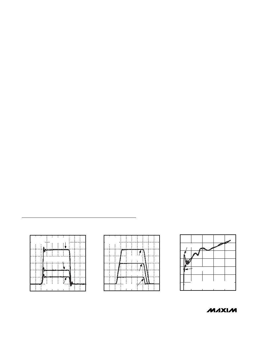
Typical Operating Characteristics
DRIVER LARGE-SIGNAL RESPONSE
MAX9961/62
toc02
V
DUT_
=
500mV/div
t = 2.50ns/div
VDLV_ = 0
RL = 50
VDHV_ = 5V
VDHV_ = 3V
VDHV_ = 1V
0
DRIVER TRAILING-EDGE TIMING ERROR
vs. PULSE WIDTH
MAX9961/62
toc03
PULSE WIDTH (ns)
TIMING
ERROR
(ps)
20
15
10
5
-80
-60
-40
-20
0
20
40
-100
025
LOW PULSE
HIGH PULSE
NORMALIZED TO PW = 12.5ns
PERIOD = 25ns, VDHV_ = 3V, VDLV_ = 0
DRIVER SMALL-SIGNAL RESPONSE
MAX9961/62
toc01
V
DUT_
=
50mV/div
t = 2.50ns/div
VDLV_ = 0
RL = 50
VDHV_ = 200mV
VDHV_ = 100mV
VDHV_ = 500mV
0
相关PDF资料 |
PDF描述 |
|---|---|
| MAX9967BRCCQ-TD | Dual, Low-Power, 500Mbps ATE Driver/Comparator with 35mA Load |
| MAX9967ADCCQ-D | Dual, Low-Power, 500Mbps ATE Driver/Comparator with 35mA Load |
| MAX9967ADCCQ-TD | Dual, Low-Power, 500Mbps ATE Driver/Comparator with 35mA Load |
| MAX9967ALCCQ-D | Dual, Low-Power, 500Mbps ATE Driver/Comparator with 35mA Load |
| MAX9967ALCCQ-TD | Dual, Low-Power, 500Mbps ATE Driver/Comparator with 35mA Load |
相关代理商/技术参数 |
参数描述 |
|---|---|
| MAX9961BLEVKIT | 功能描述:其他开发工具 RoHS:否 制造商:Parallax 产品:ELEV-8 Hex Upgrade Kits 类型:Robotics 工具用于评估:ELEV-8 Quadcopter 工作电源电压: |
| MAX9963AGCCQ+D | 功能描述:特殊用途放大器 RoHS:否 制造商:Texas Instruments 通道数量:Single 共模抑制比(最小值): 输入补偿电压: 工作电源电压:3 V to 5.5 V 电源电流:5 mA 最大功率耗散: 最大工作温度:+ 70 C 最小工作温度:- 40 C 安装风格:SMD/SMT 封装 / 箱体:QFN-20 封装:Reel |
| MAX9963AGCCQ+TD | 功能描述:特殊用途放大器 RoHS:否 制造商:Texas Instruments 通道数量:Single 共模抑制比(最小值): 输入补偿电压: 工作电源电压:3 V to 5.5 V 电源电流:5 mA 最大功率耗散: 最大工作温度:+ 70 C 最小工作温度:- 40 C 安装风格:SMD/SMT 封装 / 箱体:QFN-20 封装:Reel |
| MAX9963AGCCQ-D | 功能描述:缓冲器和线路驱动器 RoHS:否 制造商:Micrel 输入线路数量:1 输出线路数量:2 极性:Non-Inverting 电源电压-最大:+/- 5.5 V 电源电压-最小:+/- 2.37 V 最大工作温度:+ 85 C 安装风格:SMD/SMT 封装 / 箱体:MSOP-8 封装:Reel |
| MAX9963AGCCQ-TD | 功能描述:缓冲器和线路驱动器 RoHS:否 制造商:Micrel 输入线路数量:1 输出线路数量:2 极性:Non-Inverting 电源电压-最大:+/- 5.5 V 电源电压-最小:+/- 2.37 V 最大工作温度:+ 85 C 安装风格:SMD/SMT 封装 / 箱体:MSOP-8 封装:Reel |
发布紧急采购,3分钟左右您将得到回复。