- 您现在的位置:买卖IC网 > PDF目录80502 > MB89T635P-SH 8-BIT, 10 MHz, MICROCONTROLLER, PDIP64 PDF资料下载
参数资料
| 型号: | MB89T635P-SH |
| 元件分类: | 微控制器/微处理器 |
| 英文描述: | 8-BIT, 10 MHz, MICROCONTROLLER, PDIP64 |
| 封装: | SHRINK, DIP-64 |
| 文件页数: | 153/153页 |
| 文件大小: | 7326K |
| 代理商: | MB89T635P-SH |
第1页第2页第3页第4页第5页第6页第7页第8页第9页第10页第11页第12页第13页第14页第15页第16页第17页第18页第19页第20页第21页第22页第23页第24页第25页第26页第27页第28页第29页第30页第31页第32页第33页第34页第35页第36页第37页第38页第39页第40页第41页第42页第43页第44页第45页第46页第47页第48页第49页第50页第51页第52页第53页第54页第55页第56页第57页第58页第59页第60页第61页第62页第63页第64页第65页第66页第67页第68页第69页第70页第71页第72页第73页第74页第75页第76页第77页第78页第79页第80页第81页第82页第83页第84页第85页第86页第87页第88页第89页第90页第91页第92页第93页第94页第95页第96页第97页第98页第99页第100页第101页第102页第103页第104页第105页第106页第107页第108页第109页第110页第111页第112页第113页第114页第115页第116页第117页第118页第119页第120页第121页第122页第123页第124页第125页第126页第127页第128页第129页第130页第131页第132页第133页第134页第135页第136页第137页第138页第139页第140页第141页第142页第143页第144页第145页第146页第147页第148页第149页第150页第151页第152页当前第153页
MB89630 SERIES HARDWARE MANUAL
2-76
(4) Description of operation
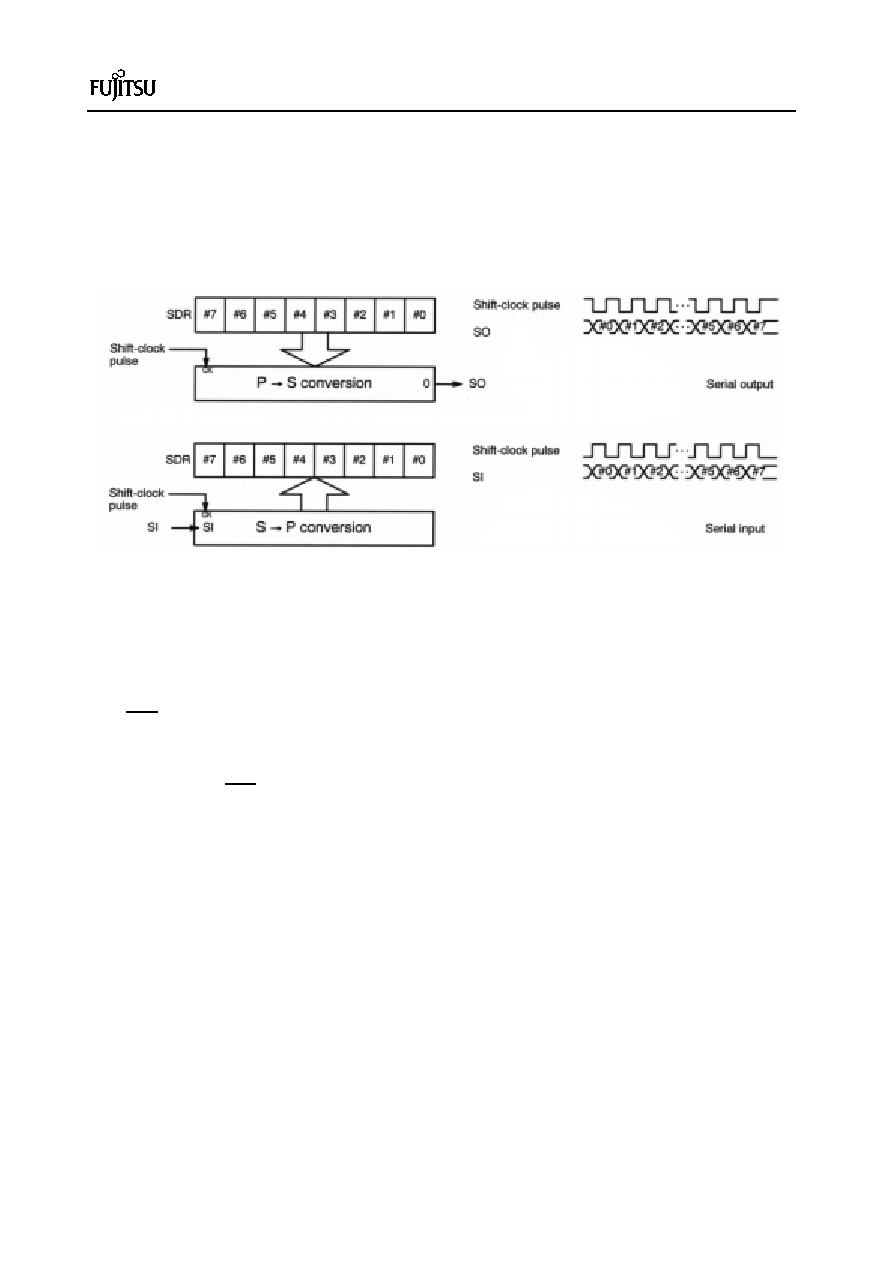
(a) Outline
This module consists of the serial-mode register (SMR) and serial-data register (SDR). At serial output,
data in the SDR is output in bit serial to the serial output pin (SO) in synchronization with the falling edge of
a serial shift-clock pulse generated from the internal or external clock. At serial input, data is input in bit
serial from the serial input pin (SI) to the SDR at the rising edge of a serial shift-clock pulse.
(b) Operation modes
The serial I/O has three internal shift-clock modes and one external shift-clock mode, which are specified
by the SMR. Mode switching or clock selection should be made with serial I/O stopped (SST bit (bit 0) of
SMR = 0).
(1) Internal shift-clock mode
Operation is performed by the internal clock. A shift-clock pulse with a duty of 50% is output from the
SCK pin as a synchronous timing output. Data is transferred bit-by-bit at every clock pulse.
(2) External shift-clock mode
Data is transferred bit-by-bit at every clock pulse in synchronization with the external shift-clock pulse
input from the SCK pin. If an external clock is input when the SST bit is set to 0, no shift operation
occurs and data of the SDR register (or the value of bit 7 when MSB first used) is output to the SO
pin. However, the pin value is also rewritten when the SDR register data is rewritten. The transfer
speed can be from DC to 1/2 oscillation (two instruction cycles). When one instruction cycle is 0.4
s
(at 10 MHz oscilla tion), the transfer speed can be up to 1.25 MHz.
Do not write data to the SMR and SDR during the serial I/O operation in either mode.
相关PDF资料 |
PDF描述 |
|---|---|
| MB89195PF | 8-BIT, MROM, 4.2 MHz, MICROCONTROLLER, PDSO28 |
| MB89152APF | 8-BIT, MROM, MICROCONTROLLER, PQFP80 |
| MB89P155PF-105 | 8-BIT, OTPROM, MICROCONTROLLER, PQFP80 |
| MD2202-D192 | FLASH MEMORY DRIVE CONTROLLER, PDIP32 |
| M38022M4-XXXSP | 8-BIT, MROM, MICROCONTROLLER, PDIP64 |
相关代理商/技术参数 |
参数描述 |
|---|---|
| MB89T637R-101P-G-SH | 制造商:FUJITSU 功能描述: |
| MB89T637R-102P-G-SH-E1 | 制造商:FUJITSU 功能描述: |
| MB89T715APF-G-BND-T | 制造商:FUJITSU 功能描述: |
| MB8A3A2HR | 制造商:Kessler-Ellis Products 功能描述: |
| MB8AA0510RBC-GE1 | 功能描述:IC 10 GIGABIT ETHER INTER RoHS:是 类别:集成电路 (IC) >> 接口 - 电信 系列:- 产品培训模块:Lead (SnPb) Finish for COTS 产品变化通告:Product Discontinuation 06/Feb/2012 标准包装:750 系列:* |
发布紧急采购,3分钟左右您将得到回复。