- 您现在的位置:买卖IC网 > PDF目录8751 > MC100ES6226AC (IDT, Integrated Device Technology Inc)IC CLK BUFF DVDR 1:9 3GHZ 32LQFP PDF资料下载
参数资料
| 型号: | MC100ES6226AC |
| 厂商: | IDT, Integrated Device Technology Inc |
| 文件页数: | 6/9页 |
| 文件大小: | 0K |
| 描述: | IC CLK BUFF DVDR 1:9 3GHZ 32LQFP |
| 标准包装: | 250 |
| 系列: | 100ES |
| 类型: | 扇出缓冲器(分配),除法器 |
| 电路数: | 1 |
| 比率 - 输入:输出: | 1:9 |
| 差分 - 输入:输出: | 是/是 |
| 输入: | LVCMOS,LVPECL |
| 输出: | LVPECL |
| 频率 - 最大: | 3GHz |
| 电源电压: | 2.375 V ~ 3.465 V |
| 工作温度: | 0°C ~ 110°C |
| 安装类型: | 表面贴装 |
| 封装/外壳: | 32-LQFP |
| 供应商设备封装: | 32-TQFP(7x7) |
| 包装: | 托盘 |
| 其它名称: | 800-2002 MC100ES6226ACIDT-ND |
MC100ES6226 REVESION 5 DECEMBER 18, 2012
6
2012 Integrated Device Technology, Inc.
MC100ES6226 Data Sheet
2.5V/3.3V DIFFERENTIAL LVPECL 1:9 CLOCK DISTRIBUTION BUFFER AND CLOCK DRIVER
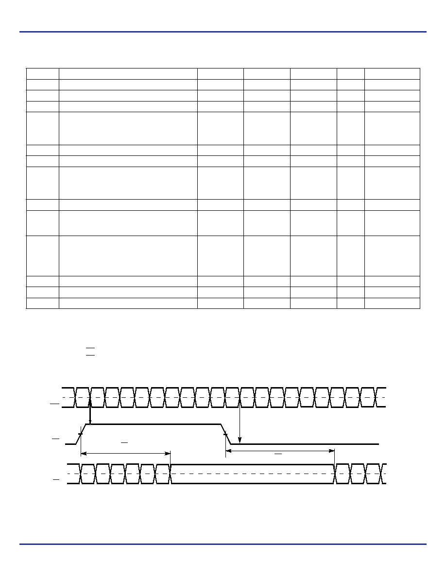
Figure 3. MC100ES6226 Output Disable/Enable Timing
Table 7. AC Characteristics (VCC = 3.3V ± 5% and 2.5V ± 5%, TJ = 0°C to +110°C)(1)
1. AC characteristics apply for parallel output termination of 50
to VTT.
Symbol
Characteristics
Min
Typ
Max
Unit
Condition
VPP
Differential Input Voltage(2) (peak-to-peak)
2. VPP is the minimum differential input voltage swing required to maintain AC characteristics including tpd and device-to-device skew.
0.2
0.3
1.3
V
VCMR
Differential Input Crosspoint Voltage(3)
3. VCMR (AC) is the crosspoint of the differential input signal. Normal AC operation is obtained when the crosspoint is within the VCMR (AC) range and the
input swing lies within the VPP (AC) specification. Violation of VCMR (AC) or VPP (AC) impacts the device propagation delay, device and part-to-part skew.
1.0
VCC – 0.3
V
VX,OUT
Differential Output Crosspoint Voltage
VCC – 1.45
VCC – 1.1
V
VO(P-P)
Differential Output Voltage (peak-to-peak)
fO < 300MHz
fO < 1.5GHz
fO < 2.7GHz
0.45
0.3
TBD
0.72
0.55
0.37
0.95
V
fCLK
Input Frequency
0
3000(4)
4. The MC100ES6226 is fully operational up to 3.0GHz and is characterized up to 2.7GHz.
MHz
tPD
Propagation Delay CLK to Qx[]
475
500
800
ps
Differential
tsk(O)
Output-to-Output Skew
(within QA[2:0])
(within QB[2:0])
(within QC[2:0])
(within device)
11
12
4
25
20
60
ps
Differential
tsk(PP)
Output-to-Output Skew
(part-to-part)
325
ps
Differential
tJIT(CC)
Output Cycle-to-Cycle Jitter
RMS (1
)
single frequency configuration
1/2 frequency configuration
1
ps
FSEL0 = FSEL1
FSEL0
FSEL1
DCO
Output Duty Cycle
Qx =
1, fO < 300MHz
Qx =
1, fO > 300MHz
Qx =
2, fO < 300MHz
Qx =
2, fO > 300MHz
48
45
49
47.5
50
52
55
51
52.5
%
DCfref = 50%
tr, tf
Output Rise/Fall Time
0.05
200
ns
20% to 80%
tPDL(5)
5. Propagation delay OE de-assertion to differential output disabled (differential low: true output low, complementary output high).
Output Disable Time
2.5
T + tPD
4.5
T + tPD
ns
T = CLK period
tPLD(6)
6. Propagation delay OE assertion to output enabled (active).
Output Enable Time
3
T + tPD
5
T + tPD
ns
T = CLK period
tPDL (OE to Qx)
50%
tPLD (OE to Qx)
Outputs Disabled
CLK
OE
Qx
相关PDF资料 |
PDF描述 |
|---|---|
| SY10E160JZ | IC PARITY GEN/CHKER 12BIT 28PLCC |
| ICS8535AG-31LF | IC CLOCK BUFFER MUX 2:4 20-TSSOP |
| ICS8533AG-01LF | IC CLOCK BUFFER MUX 2:4 20-TSSOP |
| VE-26V-MW-F4 | CONVERTER MOD DC/DC 5.8V 100W |
| VE-JNJ-MZ-F1 | CONVERTER MOD DC/DC 36V 25W |
相关代理商/技术参数 |
参数描述 |
|---|---|
| MC100ES6226ACR2 | 功能描述:时钟驱动器及分配 FSL 1-9 Diff LVPECL Clk Div Fanout Buff. RoHS:否 制造商:Micrel 乘法/除法因子:1:4 输出类型:Differential 最大输出频率:4.2 GHz 电源电压-最大: 电源电压-最小:5 V 最大工作温度:+ 85 C 封装 / 箱体:SOIC-8 封装:Reel |
| MC100ES6226FA | 功能描述:时钟缓冲器 Buffer RoHS:否 制造商:Texas Instruments 输出端数量:5 最大输入频率:40 MHz 传播延迟(最大值): 电源电压-最大:3.45 V 电源电压-最小:2.375 V 最大功率耗散: 最大工作温度:+ 85 C 最小工作温度:- 40 C 封装 / 箱体:LLP-24 封装:Reel |
| MC100ES6254AC | 功能描述:时钟驱动器及分配 FSL Differential LVP ECL 2x2 Clock Switch RoHS:否 制造商:Micrel 乘法/除法因子:1:4 输出类型:Differential 最大输出频率:4.2 GHz 电源电压-最大: 电源电压-最小:5 V 最大工作温度:+ 85 C 封装 / 箱体:SOIC-8 封装:Reel |
| MC100ES6254ACR2 | 功能描述:时钟驱动器及分配 FSL Differential LVP ECL 2x2 Clock Switch RoHS:否 制造商:Micrel 乘法/除法因子:1:4 输出类型:Differential 最大输出频率:4.2 GHz 电源电压-最大: 电源电压-最小:5 V 最大工作温度:+ 85 C 封装 / 箱体:SOIC-8 封装:Reel |
| MC100ES6254FA | 功能描述:时钟缓冲器 Buffer RoHS:否 制造商:Texas Instruments 输出端数量:5 最大输入频率:40 MHz 传播延迟(最大值): 电源电压-最大:3.45 V 电源电压-最小:2.375 V 最大功率耗散: 最大工作温度:+ 85 C 最小工作温度:- 40 C 封装 / 箱体:LLP-24 封装:Reel |
发布紧急采购,3分钟左右您将得到回复。