- 您现在的位置:买卖IC网 > PDF目录69024 > MC12430FA (INTEGRATED DEVICE TECHNOLOGY INC) 800 MHz, OTHER CLOCK GENERATOR, PQFP32 PDF资料下载
参数资料
| 型号: | MC12430FA |
| 厂商: | INTEGRATED DEVICE TECHNOLOGY INC |
| 元件分类: | 时钟产生/分配 |
| 英文描述: | 800 MHz, OTHER CLOCK GENERATOR, PQFP32 |
| 封装: | PLASTIC, LQFP-32 |
| 文件页数: | 8/12页 |
| 文件大小: | 503K |
| 代理商: | MC12430FA |
MC12430
5
MOTOROLA
be 16.666 MHz. From this reference, one can generate a
family of output frequencies at multiples of the 33.333 MHz
PCI clock. As an example, to generate a 133.333 MHz clock
from a 16.666 MHz reference, the following M and N values
would be used:
FOUT = 16.666
÷ 16 x M x 2 ÷ N = 1.04166 x M x 2 ÷ N
Let N = 4, M = 133.3333
÷ 1.04166 x 2 = 256
The value for M falls within the constraints set for PLL stability,
therefore, N[1:0] = 01 and M[8:0] = 10000000. If the value for
M fell outside of the valid range, a different N value would be
selected to try to move M in the appropriate direction.
The M and N counters can be loaded either through a
parallel or serial interface. The parallel interface is controlled
via the P_LOAD signal such that a LOW to HIGH transition will
latch the information present on the M[8:0] and N[1:0] inputs
into the M and N counters. When the P_LOAD signal is LOW,
the input latches will be transparent and any changes on the
M[8:0] and N[1:0] inputs will affect the FOUT output pair. To
use the serial port, the S_CLOCK signal samples the
information on the S_DATA line and loads it into a 14 bit shift
register. Note that the P_LOAD signal must be HIGH for the
serial load operation to function. The Test register is loaded
with the first three bits, the N register with the next two and the
M register with the final eight bits of the data stream on the
S_DATA input. For each register, the most significant bit is
loaded first (T2, N1 and M8). A pulse on the S_LOAD pin after
the shift register is fully loaded will transfer the divide values
into the counters. The HIGH to LOW transition on the S_LOAD
input will latch the new divide values into the counters.
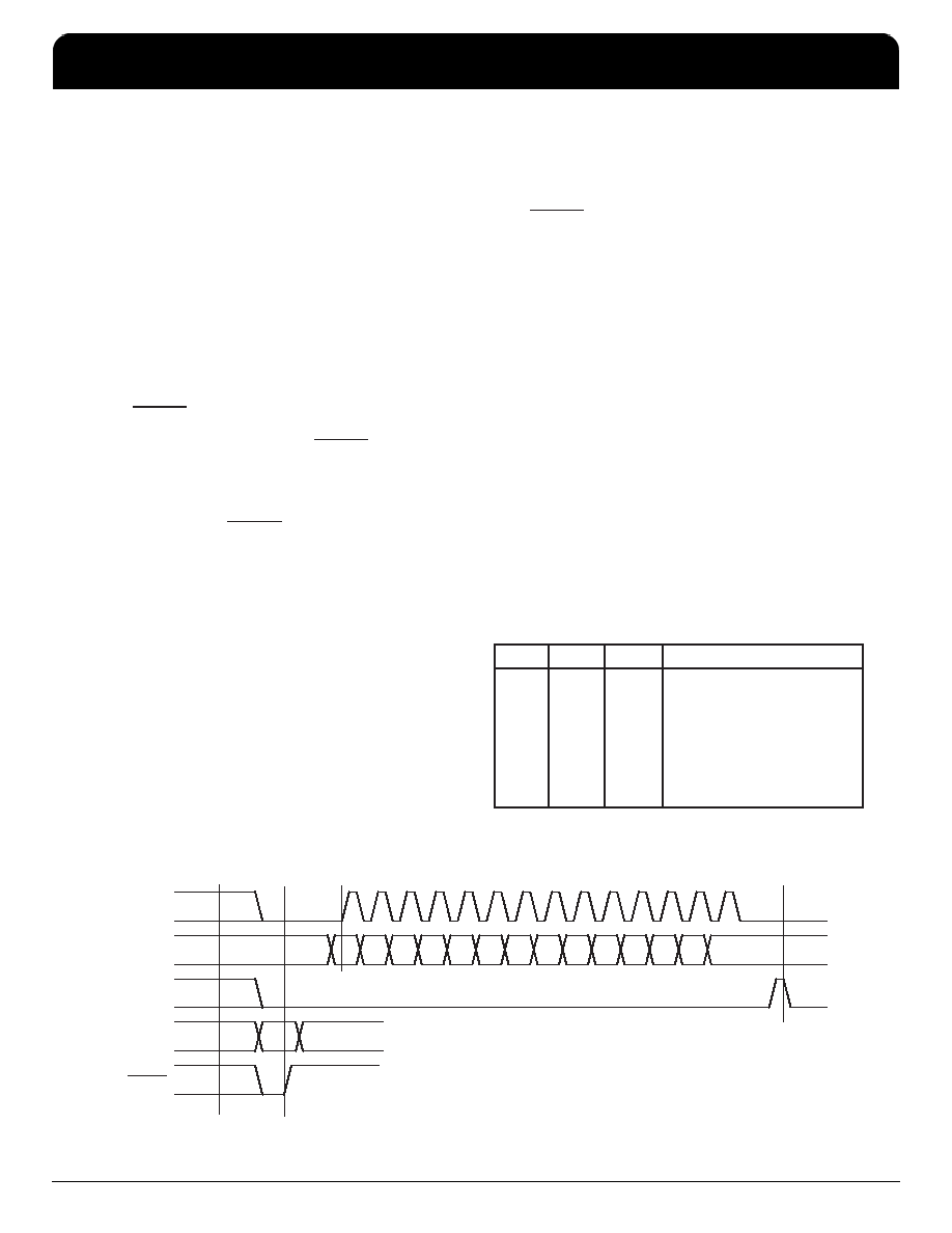
Figure 4 illustrates the timing diagram for both a parallel and a
serial load of the MC12430 synthesizer.
M[8:0] and N[1:0] are normally specified once at power–up
through the parallel interface, and then possibly again through
the serial interface. This approach allows the application to
come up at one frequency and then change or fine–tune the
clock as the ability to control the serial interface becomes
available.
The TEST output provides visibility for one of the several
internal nodes as determined by the T[2:0] bits in the serial
configuration stream. It is not configurable through the parallel
interface. The T2, T1 and T0 control bits are preset to ‘000’
when P_LOAD is LOW so that the PECL FOUT outputs are as
jitter–free as possible. Any active signal on the TEST output
pin will have detrimental affects on the jitter of the PECL output
pair. In normal operations, jitter specifications are only
guaranteed if the TEST output is static. The serial
configuration port can be used to select one of the alternate
functions for this pin.
Most of the signals available on the TEST output pin are
useful only for performance verification of the MC12430 itself.
However, the PLL bypass mode may be of interest at the
board level for functional debug. When T[2:0] is set to 110 the
MC12430 is placed in PLL bypass mode. In this mode the
S_CLOCK input is fed directly into the M and N dividers. The N
divider drives the FOUT differential pair and the M counter
drives the TEST output pin. In this mode the S_CLOCK input
could be used for low speed board level functional test or
debug. Bypassing the PLL and driving FOUT directly gives the
user more control on the test clocks sent through the clock
tree. Figure 5 shows the functional setup of the PLL bypass
mode. Because the S_CLOCK is a CMOS level, the input
frequency is limited to 250 MHz or less. This means the fastest
the FOUT pin can be toggled via the S_CLOCK is 250MHz as
the minimum divide ratio of the N counter is 1. Note that the M
counter output on the TEST output will not be a 50% duty cycle
due to the way the divider is implemented.
T2
T1
T0
TEST (Pin 20)
0
1
0
1
0
1
0
1
0
1
0
1
0
1
SHIFT REGISTER OUT
HIGH
FREF
M COUNTER OUT/2
FOUT
LOW
M COUNTER/2 in
PLL Bypass Mode
FOUT/4
Figure 4. Timing Diagram
S_CLOCK
S_DATA
S_LOAD
M[8:0]
N[1:0]
P_LOAD
T2
T1
T0
N1
N0
M8 M7 M6 M5 M4 M3 M2 M1
M0
M, N
First
Bit
Last
Bit
F
re
e
sc
a
le
S
e
m
ic
o
n
d
u
c
to
r,
I
Freescale Semiconductor, Inc.
For More Information On This Product,
Go to: www.freescale.com
n
c
..
.
MC12430
High Frequency Clock Synthesizer
NETCOM
IDT High Frequency Clock Synthesizer
Freescale Timing Solutions Organization has been acquired by Integrated Device Technology, Inc
MC12430
5
相关PDF资料 |
PDF描述 |
|---|---|
| MC13214R2 | SPECIALTY MICROPROCESSOR CIRCUIT, BGA71 |
| MC13224VR2 | SPECIALTY MICROPROCESSOR CIRCUIT, PBGA99 |
| MC13226V | SPECIALTY MICROPROCESSOR CIRCUIT, PBGA99 |
| MC13226VR2 | SPECIALTY MICROPROCESSOR CIRCUIT, PBGA99 |
| MC13224V | SPECIALTY MICROPROCESSOR CIRCUIT, PBGA99 |
相关代理商/技术参数 |
参数描述 |
|---|---|
| MC12430FN | 制造商:MOTOROLA 制造商全称:Motorola, Inc 功能描述:HIGH FREQUENCY PLL CLOCK GENERATOR |
| MC12439 | 制造商:MOTOROLA 制造商全称:Motorola, Inc 功能描述:HIGH FREQUENCY PLL CLOCK GENERATOR |
| MC12439FN | 制造商:Motorola Inc 功能描述: 制造商:Motorola Inc 功能描述:MISCELLANEOUS CLOCK GENERATOR, 28 Pin, Plastic, PLCC |
| MC1243F | 制造商:Rochester Electronics LLC 功能描述:- Bulk |
| MC1245L | 制造商:Rochester Electronics LLC 功能描述:- Bulk |
发布紧急采购,3分钟左右您将得到回复。