- 您现在的位置:买卖IC网 > PDF目录371008 > MC1311 (Motorola, Inc.) UNIVERSAL NARROWBAND FM RECEIVER INTEGRATED CIRCUIT PDF资料下载
参数资料
| 型号: | MC1311 |
| 厂商: | Motorola, Inc. |
| 英文描述: | UNIVERSAL NARROWBAND FM RECEIVER INTEGRATED CIRCUIT |
| 中文描述: | 通用窄带调频接收器集成电路 |
| 文件页数: | 40/68页 |
| 文件大小: | 1316K |
| 代理商: | MC1311 |
第1页第2页第3页第4页第5页第6页第7页第8页第9页第10页第11页第12页第13页第14页第15页第16页第17页第18页第19页第20页第21页第22页第23页第24页第25页第26页第27页第28页第29页第30页第31页第32页第33页第34页第35页第36页第37页第38页第39页当前第40页第41页第42页第43页第44页第45页第46页第47页第48页第49页第50页第51页第52页第53页第54页第55页第56页第57页第58页第59页第60页第61页第62页第63页第64页第65页第66页第67页第68页
MC13110A/B MC13111A/B
40
MOTOROLA ANALOG IC DEVICE DATA
Loop Filter Characteristics
Lets consider the following discussion on loop filters. The
fundamental loop characteristics, such as capture range,
loop bandwidth, lock–up time, and transient response are
controlled externally by loop filtering.
Figure 96 is the general model for a Phase Lock Loop
(PLL).
Phase
Detector (Kpd)
Filter
(Kf)
VCO
(Ko)
fo
Divider
(Kn)
fi
Figure 96. PLL Model
Where:
Kpd = Phase Detector Gain Constant
Kf = Loop Filter Transfer Function
Ko = VCO Gain Constant
Kn = Divide Ratio (1/N)
fi = Input frequency
fo = Output frequency
fo/N = Feedback frequency divided by N
From control theory the loop transfer function can be
represented as follows:
A = Kpd Kf Ko Kn Open loop gain
Kpd can be either expressed as being 2.5 V/4.0
π
or
1.0 mA/2.0
π
for the CT–0 circuits. More details about
performance of different type PLL loops, refer to Motorola
application note AN535.
The loop filter can take the form of a simple low pass filter.
A current output, type 2 filter will be used in this discussion
since it has the advantage of improved step response,
velocity, and acceleration.
The type 2 low pass filter discussed here is represented as
follows:
From
Phase
Detector
To VCO
R2
C2
C1
Figure 97. Loop Filter
with Additional Integrating Element
From Figure 97, capacitor C1 forms an additional
integrator, providing the type 2 response, and filters the
discrete current steps from the phase detector output. The
function of the additional components R2 and C2 is to create
a pole and a zero (together with C1) around the 0 dB point of
the open loop gain. This will create sufficient phase margin
for stable loop operation.
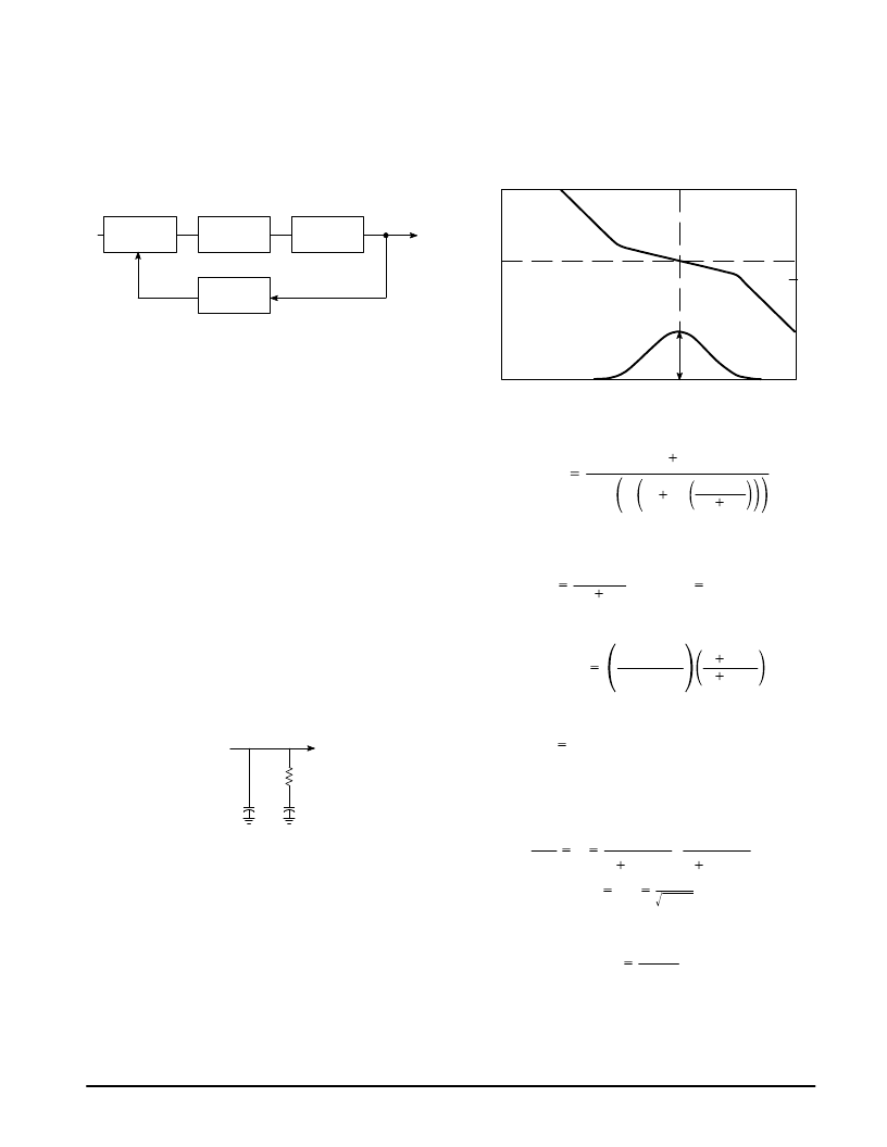
In Figure 98, the open loop gain and the phase is
displayed in the form of a Bode plot. Since there are two
integrating functions in the loop, originating from the loopfilter
and the VCO gain, the open loop gain response follows a
second order slope (–40 dB/dec) creating a phase of –180
degrees at the lower and higher frequencies. The filter
characteristic needs to be determined such that it is adding a
pole and a zero around the 0 dB point to guarantee sufficient
phase margin in this design (Qp in Figure 98).
Phase
Figure 98. Bode Plot of Gain and
Phase in Open Loop Condition
A
wp
Open Loop Gain
Qp
–180
–90
0
0
The open loop gain including the filter response can be
expressed as:
Aopenloop
KpdKo(1
jw(R2C2)
)
jwKnjw 1
jwC1
C2
(1)
The two time constants creating the pole and the zero in
the Bode plot can now be defined as:
T1
R2C1C2
C1
C2
T2
R2C2
(2)
By substituting equation (2) into (1), it follows:
Aopenloop
KpdKoT1
w2C1KnT2
1
1
jwT2
jwT1
(3)
The phase margin (phase + 180) is thus determined by:
Qp
arctan(wT2)–arctan(wT1)
(4)
At w=wp, the derivative of the phase margin may be set to
zero in order to assure maximum phase margin occurs at wp
(see also Figure 98). This provides an expression for wp:
dQp
dw
0
T2
1
T1
(wT1)2
1
(5)
w
wp
1
T2T1
(6)
Or rewritten:
T1
1
wp2T2
(7)
相关PDF资料 |
PDF描述 |
|---|---|
| MC13110AFB | UNIVERSAL NARROWBAND FM RECEIVER INTEGRATED CIRCUIT |
| MC13110AFTA | UNIVERSAL NARROWBAND FM RECEIVER INTEGRATED CIRCUIT |
| MC13110BFB | UNIVERSAL NARROWBAND FM RECEIVER INTEGRATED CIRCUIT |
| MC13111AFB | UNIVERSAL NARROWBAND FM RECEIVER INTEGRATED CIRCUIT |
| MC13110BFTA | UNIVERSAL NARROWBAND FM RECEIVER INTEGRATED CIRCUIT |
相关代理商/技术参数 |
参数描述 |
|---|---|
| MC13110 | 制造商:MOTOROLA 制造商全称:Motorola, Inc 功能描述:UNIVERSAL NARROWBAND FM RECEIVER INTEGRATED CIRCUIT |
| MC13110A | 制造商:MOTOROLA 制造商全称:Motorola, Inc 功能描述:UNIVERSAL CORDLESS TELEPHONE SUBSYSTEM IC |
| MC13110AFB | 制造商:MOTOROLA 制造商全称:Motorola, Inc 功能描述:UNIVERSAL CORDLESS TELEPHONE SUBSYSTEM IC |
| MC13110AFTA | 制造商:MOTOROLA 制造商全称:Motorola, Inc 功能描述:UNIVERSAL NARROWBAND FM RECEIVER INTEGRATED CIRCUIT |
| MC13110BFB | 制造商:MOTOROLA 制造商全称:Motorola, Inc 功能描述:UNIVERSAL NARROWBAND FM RECEIVER INTEGRATED CIRCUIT |
发布紧急采购,3分钟左右您将得到回复。