- 您现在的位置:买卖IC网 > PDF目录371008 > MC1311 (Motorola, Inc.) UNIVERSAL NARROWBAND FM RECEIVER INTEGRATED CIRCUIT PDF资料下载
参数资料
| 型号: | MC1311 |
| 厂商: | Motorola, Inc. |
| 英文描述: | UNIVERSAL NARROWBAND FM RECEIVER INTEGRATED CIRCUIT |
| 中文描述: | 通用窄带调频接收器集成电路 |
| 文件页数: | 44/68页 |
| 文件大小: | 1316K |
| 代理商: | MC1311 |
第1页第2页第3页第4页第5页第6页第7页第8页第9页第10页第11页第12页第13页第14页第15页第16页第17页第18页第19页第20页第21页第22页第23页第24页第25页第26页第27页第28页第29页第30页第31页第32页第33页第34页第35页第36页第37页第38页第39页第40页第41页第42页第43页当前第44页第45页第46页第47页第48页第49页第50页第51页第52页第53页第54页第55页第56页第57页第58页第59页第60页第61页第62页第63页第64页第65页第66页第67页第68页
MC13110A/B MC13111A/B
SERIAL PROGRAMMABLE INTERFACE
44
MOTOROLA ANALOG IC DEVICE DATA
Microprocessor Serial Interface
The Data, Clock, and Enable (“Data”, “Clk”, and “EN”
respectively) pins provide a MPU serial interface for
programming the reference counters, the transmit and
receive channel divide counters, the switched capacitor filter
clock counter, and various other control functions. The “Data”
and “Clk” pins are used to load data into the MC13111A/B
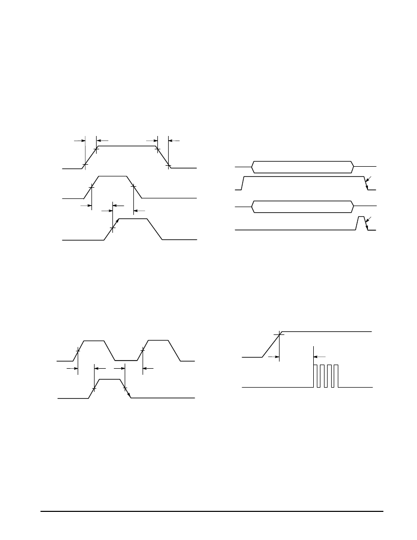
shift register (Figure 109). Figure 105 shows the timing
required on the “Data” and “Clk” pins. Data is clocked into the
shift register on positive clock transitions.
Figure 105. Data and Clock Timing Requirement
Data,
Clk, EN
Data
Clk
tsuDC
tr
tf
50%
50%
th
10%
90%
After data is loaded into the shift register, the data is
latched into the appropriate latch register using the “EN” pin.
This is done in two steps. First, an 8–bit address is loaded
into the shift register and latched into the 8–bit address latch
register. Then, up to 16–bits of data is loaded into the shift
register and latched into the data latch register. It is specified
by the address that was previously loaded. Figure 106 shows
the timing required on the EN pin. Latching occurs on the
negative EN transition.
Figure 106. Enable Timing Requirement
Clk
tsuEC
EN
50%
50%
50%
trec
Previous Data Latched
Last
Clock
First
Clock
50%
The state of the “EN” pin when clocking data into the shift
register determines whether the data is latched into the
address register or a data register. Figure 107 shows the
address and data programming diagrams. In the data
programming mode, there must not be any clock transitions
when “EN” is high. The clock can be in a high state (default
high) or a low state (default low) but must not have any
transitions during the “EN” high state. The convention in
these figures is that latch bits to the left are loaded into the
shift register first. A minimum of four “Clk” rising edge
transition must occur before a negative “EN” transition will
latch data or an address into a register.
Figure 107. Microprocessor Interface
Programming Mode Diagrams
Data
Latch
8–Bit Address
EN
Data
EN
Address Register Programming Mode
16–Bit Data
Data Register Programming Mode
Latch
Latch
MSB
MSB
LSB
LSB
The MPU serial interface is fully operational within 100
μ
s
after the power supply has reached its minimum level during
power–up (see Figure 108). The MPU Interface shift
registers and data latches are operational in all four power
saving modes; Inactive, Standby, Rx, and Active Modes.
Data can be loaded into the shift registers and latched into
the latch registers in any of the operating modes.
Figure 108. Microprocessor Serial
Interface Power–Up Delay
VCC
tpuMPU
2.7 V
Data,
Clk, EN
相关PDF资料 |
PDF描述 |
|---|---|
| MC13110AFB | UNIVERSAL NARROWBAND FM RECEIVER INTEGRATED CIRCUIT |
| MC13110AFTA | UNIVERSAL NARROWBAND FM RECEIVER INTEGRATED CIRCUIT |
| MC13110BFB | UNIVERSAL NARROWBAND FM RECEIVER INTEGRATED CIRCUIT |
| MC13111AFB | UNIVERSAL NARROWBAND FM RECEIVER INTEGRATED CIRCUIT |
| MC13110BFTA | UNIVERSAL NARROWBAND FM RECEIVER INTEGRATED CIRCUIT |
相关代理商/技术参数 |
参数描述 |
|---|---|
| MC13110 | 制造商:MOTOROLA 制造商全称:Motorola, Inc 功能描述:UNIVERSAL NARROWBAND FM RECEIVER INTEGRATED CIRCUIT |
| MC13110A | 制造商:MOTOROLA 制造商全称:Motorola, Inc 功能描述:UNIVERSAL CORDLESS TELEPHONE SUBSYSTEM IC |
| MC13110AFB | 制造商:MOTOROLA 制造商全称:Motorola, Inc 功能描述:UNIVERSAL CORDLESS TELEPHONE SUBSYSTEM IC |
| MC13110AFTA | 制造商:MOTOROLA 制造商全称:Motorola, Inc 功能描述:UNIVERSAL NARROWBAND FM RECEIVER INTEGRATED CIRCUIT |
| MC13110BFB | 制造商:MOTOROLA 制造商全称:Motorola, Inc 功能描述:UNIVERSAL NARROWBAND FM RECEIVER INTEGRATED CIRCUIT |
发布紧急采购,3分钟左右您将得到回复。