- 您现在的位置:买卖IC网 > PDF目录359132 > MC33298 (飞思卡尔半导体(中国)有限公司) Eight Output Switch with Serial Peripheral Interface I/O(带SPI接口的八输出开关) PDF资料下载
参数资料
| 型号: | MC33298 |
| 厂商: | 飞思卡尔半导体(中国)有限公司 |
| 英文描述: | Eight Output Switch with Serial Peripheral Interface I/O(带SPI接口的八输出开关) |
| 中文描述: | 8个串行外围接口的I / O(带的SPI接口的八输出开关输出开关) |
| 文件页数: | 13/28页 |
| 文件大小: | 642K |
| 代理商: | MC33298 |
第1页第2页第3页第4页第5页第6页第7页第8页第9页第10页第11页第12页当前第13页第14页第15页第16页第17页第18页第19页第20页第21页第22页第23页第24页第25页第26页第27页第28页
MOTOROLA ANALOG INTEGRATED CIRCUIT DEVICE DATA
33298
13
SYSTEM/APPLICATION INFORMATION
INTRODUCTION
The 33298 was conceived, specified, designed, and
developed for automotive applications. It is an eight output low
side power switch having 8-bit serial control. The 33298
incorporates SMARTMOS
technology having effective 1.5 μ
CMOS logic, bipolar/MOS analog circuitry, and independent
state of the art double diffused MOS (DMOS) power output
transistors. Many benefits are realized as a direct result of using
this mixed technology. A simplified block diagram delineates
33298 in Figure 1.
Where bipolar devices require considerable control current
for their operation, structured MOS devices, since they are
voltage controlled, require only transient gate charging current
affording a significant decrease in power consumption. The
CMOS capability of the SMARTMOS
process allows
significant amounts of logic to be economically incorporated
into the monolithic design. Additionally, the bipolar/MOS analog
circuits embedded within the updrain power DMOS output
transistors monitor and provide fast, independent protection
control functions for each individual output. All outputs have
internal 45 V at 0.5 A independent output voltage clamps to
provide fast inductive turn-off and transient protection.
The 33298 uses high efficiency updrain power DMOS output
transistors exhibiting very low room temperature drain-to-
source ON resistance values (R
DS(on)
≤
1.0
at 13 V V
PWR
)
and dense CMOS control logic. Operational bias currents of
less than 2.0 mA (1.0 mA typical) with any combination of
outputs ON are the result of using this mixed technology and
would not be possible with bipolar structures. To accomplish a
comparable functional feature set using a bipolar structure
approach would result in a device requiring hundreds of
milliamperes of internal bias and control current. This would
represent a very large amount of power to be consumed by the
device itself and not available for load use.
During operation, the 33298 functions as an eight output
serial switch serving as a microcontroller (MCU) bus expander
and buffer with fault management and fault reporting features.
In doing so, the device directly relieves the MCU of the fault
management functions.
The 33298 directly relieves the MCU of the fault management
functions. The 33298 directly interfaces to an MCU, operating
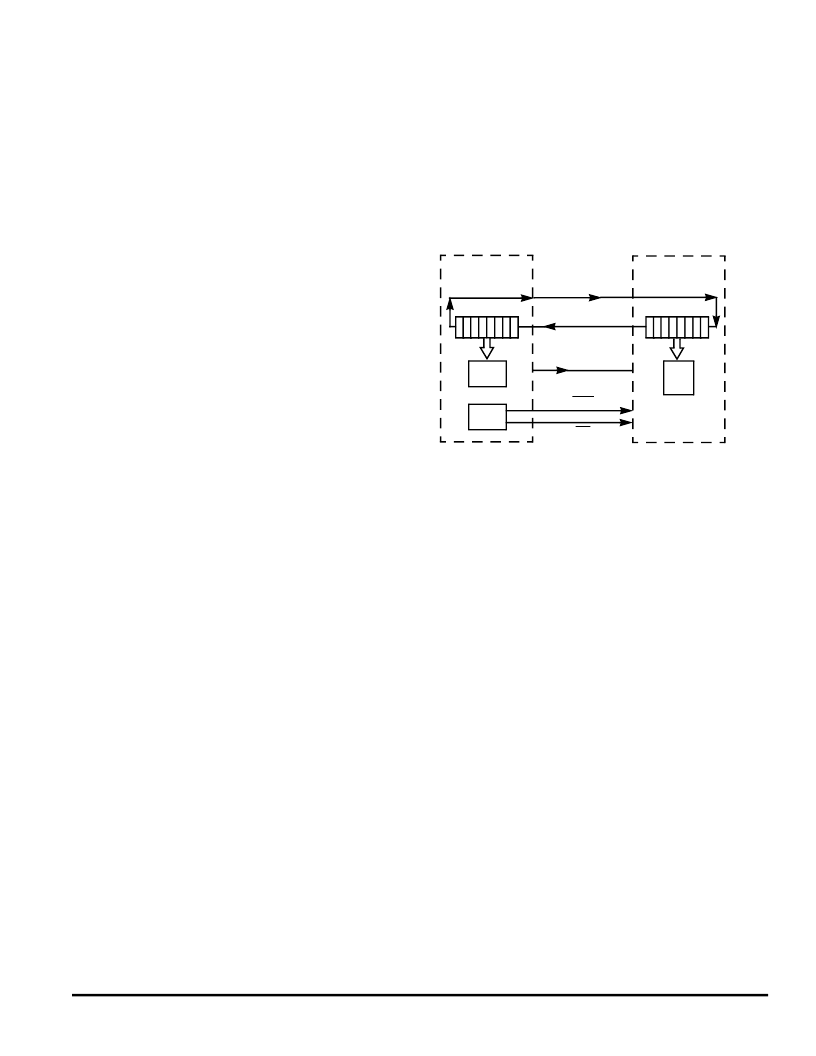
at system clock serial frequencies in excess of 3.0 MHz. It uses
a Synchronous Peripheral Interface (SPI) for control and
diagnostic readout. Figure 11 illustrates the basic SPI
configuration between an MCU and one 33298.
Figure 11. SPI Interface with Microcontroller
The circuit can also be used in a variety of other applications
in the computer, telecommunications, and industrial fields. It is
parametrically specified over an input
battery
/supply range of
9.0 to 16 V but is designed to operate over a considerably wider
range of 5.5 to 26.5 V. The design incorporates the use of Logic
Level MOSFETs as output devices. These MOSFETs are
sufficiently turned ON with a gate voltage of less than 5.0 V thus
eliminating the need for an internal charge pump. Each output
is identically sized and
independent
in operation. The efficiency
of each output transistor, at room temperature provides as little
as 9.0 V supply (V
PWR
), the maximum R
DS(on)
of an output
All inputs are compatible with 5.0 V CMOS logic levels,
incorporating negative or inverted logic. Whenever an input is
programmed to a logic low state (<1.0 V) the corresponding low
side switched output being controlled will be active low and
turned ON. Conversely, whenever an input is programmed to a
logic high state (>3.0 V), the output being controlled will be high
and turned OFF.
33298
MC68HCXX
Microcontroller
Shift Register
Shift Register
To
Logic
Receive
Buffer
Parallel
Ports
MOSI
SI
MISO
SO
SCLK
RST
CS
F
Freescale Semiconductor, Inc.
Go to: www.freescale.com
n
.
相关PDF资料 |
PDF描述 |
|---|---|
| MC33385 | QUAD LOW SIDE DRIVER(四低端驱动器) |
| MC33388 | Fault Tolerant CAN Interface(容错CAN接口) |
| MC33389 | System Basis Chip with Low Speed Fault Tolerant CAN(带低速容错CAN接口的系统基片) |
| MC33390 | J-1850 SERIAL TRANSCEIVER(串行J-1850总线收发器) |
| MC33394 | Switch Mode Power Supply with Multiple Linear Regulators and High Speed CAN Transceiver(带有多个线性稳压器和高速CAN收发器的开关方式电源) |
相关代理商/技术参数 |
参数描述 |
|---|---|
| MC33298DW | 功能描述:IC SWITCH SERIAL OCTAL 24-SOIC RoHS:否 类别:集成电路 (IC) >> PMIC - MOSFET,电桥驱动器 - 内部开关 系列:- 标准包装:1,000 系列:- 类型:高端/低端驱动器 输入类型:SPI 输出数:8 导通状态电阻:850 毫欧,1.6 欧姆 电流 - 输出 / 通道:205mA,410mA 电流 - 峰值输出:500mA,1A 电源电压:9 V ~ 16 V 工作温度:-40°C ~ 150°C 安装类型:表面贴装 封装/外壳:20-SOIC(0.295",7.50mm 宽) 供应商设备封装:PG-DSO-20-45 包装:带卷 (TR) |
| MC33298DWR2 | 功能描述:IC OCTAL SERIAL SWITCH 24-SOIC RoHS:否 类别:集成电路 (IC) >> PMIC - MOSFET,电桥驱动器 - 内部开关 系列:- 标准包装:1,000 系列:- 类型:高端/低端驱动器 输入类型:SPI 输出数:8 导通状态电阻:850 毫欧,1.6 欧姆 电流 - 输出 / 通道:205mA,410mA 电流 - 峰值输出:500mA,1A 电源电压:9 V ~ 16 V 工作温度:-40°C ~ 150°C 安装类型:表面贴装 封装/外壳:20-SOIC(0.295",7.50mm 宽) 供应商设备封装:PG-DSO-20-45 包装:带卷 (TR) |
| MC33298P | 功能描述:IC SWITCH SERIAL OCTAL 20-DIP RoHS:否 类别:集成电路 (IC) >> PMIC - MOSFET,电桥驱动器 - 内部开关 系列:- 标准包装:1,000 系列:- 类型:高端/低端驱动器 输入类型:SPI 输出数:8 导通状态电阻:850 毫欧,1.6 欧姆 电流 - 输出 / 通道:205mA,410mA 电流 - 峰值输出:500mA,1A 电源电压:9 V ~ 16 V 工作温度:-40°C ~ 150°C 安装类型:表面贴装 封装/外壳:20-SOIC(0.295",7.50mm 宽) 供应商设备封装:PG-DSO-20-45 包装:带卷 (TR) |
| MC33304P | 制造商:ON Semiconductor 功能描述: |
| MC3330P | 制造商:Rochester Electronics LLC 功能描述:- Bulk |
发布紧急采购,3分钟左右您将得到回复。