- 您现在的位置:买卖IC网 > PDF目录359132 > MC33298 (飞思卡尔半导体(中国)有限公司) Eight Output Switch with Serial Peripheral Interface I/O(带SPI接口的八输出开关) PDF资料下载
参数资料
| 型号: | MC33298 |
| 厂商: | 飞思卡尔半导体(中国)有限公司 |
| 英文描述: | Eight Output Switch with Serial Peripheral Interface I/O(带SPI接口的八输出开关) |
| 中文描述: | 8个串行外围接口的I / O(带的SPI接口的八输出开关输出开关) |
| 文件页数: | 15/28页 |
| 文件大小: | 642K |
| 代理商: | MC33298 |
第1页第2页第3页第4页第5页第6页第7页第8页第9页第10页第11页第12页第13页第14页当前第15页第16页第17页第18页第19页第20页第21页第22页第23页第24页第25页第26页第27页第28页
MOTOROLA ANALOG INTEGRATED CIRCUIT DEVICE DATA
33298
15
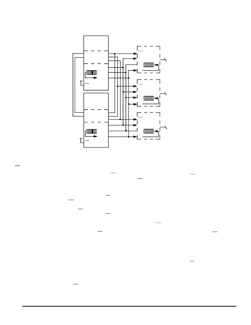
Figure 14. Multiple MCU SPI Control
FUNCTIONAL PIN DESCRIPTION
CS Pin
The 33298 receives its MCU communication through the CS
pin. Whenever this pin is in a logic low state, data can be
transferred from the MCU to the 33298 by way of the SI pin and
from the 33298 to the MCU through the SO pin. Clocked-in data
from the MCU is transferred from the 33298 Shift register and
latched into the power outputs on the rising edge of the CS
signal. On the falling edge of the CS signal, drain status
information is transferred from the power outputs then loaded
into the Shift register of the device. The CS pin also controls the
output driver of the serial output (SO) pin. Whenever the CS pin
goes to a logic low state, the SO pin output driver is enabled
allowing information to be transferred from the 33298 to the
MCU. To avoid data corruption or the generation of spurious
data, it is essential the high-to-low transition of the CS signal
occur only when SCLK is in a logic low state.
SCLK Pin
The system clock (SCLK) pin clocks the internal shift
registers of the 33298. The serial input (SI) pin accepts data into
the Input Shift register on the falling edge of the SCLK signal
while the serial output (SO) pin shifts data information out of the
SO line driver on the rising edge of the SCLK signal. False
clocking of the Shift register must be avoided to guarantee
validity of data. It is essential the SCLK pin be in a logic low
state whenever the chip select bar (CS) pin makes any
transition. For this reason, it is recommended, though not
absolutely necessary, the SCLK pin be kept in a low logic state
as long as the device is not accessed (CS in logic high state).
When CS is in a logic high state, signals at the SCLK and SI
pins are ignored and SO is tri-stated (high impedance). See the
Data Transfer Timing diagram in Figure 16.
SI Pin
This pin is for the input of serial instruction (SI) data. SI is
read on the falling edge of SCLK. A logic high state present on
this pin when the SCLK signal rises will program a specific
output OFF. In turn, the pin turns OFF the specific output on the
rising edge of the CS signal. Conversely, a logic low state
present on the SI pin will program the output ON, In turn, the pin
turns ON the specific output on the rising edge of the CS signal.
To program the eight outputs of the 33298 ON or OFF, an 8-
bit serial stream of data is required to be synchronously entered
into the SI pin starting with Output 7, followed by Output 6,
Output 5, and so on, to Output 0. Referring to Figure 15, the DO
bit is the most significant bit (MSB) corresponding to Output 7.
For each rise of the SCLK signal, with CS held in a logic low
state, a data-bit instruction (ON or OFF) is synchronously
loaded into the Shift register per the data-bit SI state. The Shift
register is full after eight bits of information have been entered.
To preserve data integrity, care should be taken to not transition
SI as SCLK transitions from a low-to-high logic state.
SI
SO
SCLK
CS
8-Bit
33298
SI
SO
SCLK
CS
8-Bit
33298
SI
SO
SCLK
CS
8-Bit
33298
8 Outputs
8 Outputs
8 Outputs
V
DD
V
DD
B0
B1
B0
B1
MC68XX
Microcontroller
SPI
(Master)
A0
A1
A2
A0
A1
A2
MC68XX
Microcontroller
SPI
(Alternate Master)
Parallel
Ports
8-Bit
Parallel
Ports
SCLK
MISO
MOSI
SCLK
MISO
MOSI
SS
SS
8-Bit
F
Freescale Semiconductor, Inc.
Go to: www.freescale.com
n
.
相关PDF资料 |
PDF描述 |
|---|---|
| MC33385 | QUAD LOW SIDE DRIVER(四低端驱动器) |
| MC33388 | Fault Tolerant CAN Interface(容错CAN接口) |
| MC33389 | System Basis Chip with Low Speed Fault Tolerant CAN(带低速容错CAN接口的系统基片) |
| MC33390 | J-1850 SERIAL TRANSCEIVER(串行J-1850总线收发器) |
| MC33394 | Switch Mode Power Supply with Multiple Linear Regulators and High Speed CAN Transceiver(带有多个线性稳压器和高速CAN收发器的开关方式电源) |
相关代理商/技术参数 |
参数描述 |
|---|---|
| MC33298DW | 功能描述:IC SWITCH SERIAL OCTAL 24-SOIC RoHS:否 类别:集成电路 (IC) >> PMIC - MOSFET,电桥驱动器 - 内部开关 系列:- 标准包装:1,000 系列:- 类型:高端/低端驱动器 输入类型:SPI 输出数:8 导通状态电阻:850 毫欧,1.6 欧姆 电流 - 输出 / 通道:205mA,410mA 电流 - 峰值输出:500mA,1A 电源电压:9 V ~ 16 V 工作温度:-40°C ~ 150°C 安装类型:表面贴装 封装/外壳:20-SOIC(0.295",7.50mm 宽) 供应商设备封装:PG-DSO-20-45 包装:带卷 (TR) |
| MC33298DWR2 | 功能描述:IC OCTAL SERIAL SWITCH 24-SOIC RoHS:否 类别:集成电路 (IC) >> PMIC - MOSFET,电桥驱动器 - 内部开关 系列:- 标准包装:1,000 系列:- 类型:高端/低端驱动器 输入类型:SPI 输出数:8 导通状态电阻:850 毫欧,1.6 欧姆 电流 - 输出 / 通道:205mA,410mA 电流 - 峰值输出:500mA,1A 电源电压:9 V ~ 16 V 工作温度:-40°C ~ 150°C 安装类型:表面贴装 封装/外壳:20-SOIC(0.295",7.50mm 宽) 供应商设备封装:PG-DSO-20-45 包装:带卷 (TR) |
| MC33298P | 功能描述:IC SWITCH SERIAL OCTAL 20-DIP RoHS:否 类别:集成电路 (IC) >> PMIC - MOSFET,电桥驱动器 - 内部开关 系列:- 标准包装:1,000 系列:- 类型:高端/低端驱动器 输入类型:SPI 输出数:8 导通状态电阻:850 毫欧,1.6 欧姆 电流 - 输出 / 通道:205mA,410mA 电流 - 峰值输出:500mA,1A 电源电压:9 V ~ 16 V 工作温度:-40°C ~ 150°C 安装类型:表面贴装 封装/外壳:20-SOIC(0.295",7.50mm 宽) 供应商设备封装:PG-DSO-20-45 包装:带卷 (TR) |
| MC33304P | 制造商:ON Semiconductor 功能描述: |
| MC3330P | 制造商:Rochester Electronics LLC 功能描述:- Bulk |
发布紧急采购,3分钟左右您将得到回复。