- 您现在的位置:买卖IC网 > PDF目录45205 > MC33780EGR2 (FREESCALE SEMICONDUCTOR INC) SPECIALTY MICROPROCESSOR CIRCUIT, PDSO16 PDF资料下载
参数资料
| 型号: | MC33780EGR2 |
| 厂商: | FREESCALE SEMICONDUCTOR INC |
| 元件分类: | 微控制器/微处理器 |
| 英文描述: | SPECIALTY MICROPROCESSOR CIRCUIT, PDSO16 |
| 封装: | 1.27 MM PITCH, ROHS COMPLIANT, SOIC-16 |
| 文件页数: | 11/37页 |
| 文件大小: | 851K |
| 代理商: | MC33780EGR2 |
第1页第2页第3页第4页第5页第6页第7页第8页第9页第10页当前第11页第12页第13页第14页第15页第16页第17页第18页第19页第20页第21页第22页第23页第24页第25页第26页第27页第28页第29页第30页第31页第32页第33页第34页第35页第36页第37页
Analog Integrated Circuit Device Data
Freescale Semiconductor
19
33780
FUNCTIONAL DEVICE OPERATION
LOGIC COMMANDS AND REGISTERS
FUNCTIONAL DEVICE OPERATION
LOGIC COMMANDS AND REGISTERS
SPI COMMUNICATIONS
All SPI transactions start with a command byte and can be
followed by 1 or more bytes of data. The start of an SPI
transaction is signaled by CS being asserted low. The first bit
sent (bit 7) of the first byte signals a read or write (write = 1)
of data. The last five bits (bits 4–0) of the command set a
pointer to the desired register. Bits 5 and 6 are unused. See
sent over the SPI will be a read/write of data to the sequential
next register. After address 10101 is written to, the next write
will wrap around to address 00000.
Figure 13. SPI Communications, First Byte of Burst Transfer
The receive FIFO is popped only when the SPI reads or
writes the low data register (DnL). The Control and Status
registers can be read without affecting the receive FIFO. The
transmit FIFO is popped at the end of the DBUS transaction.
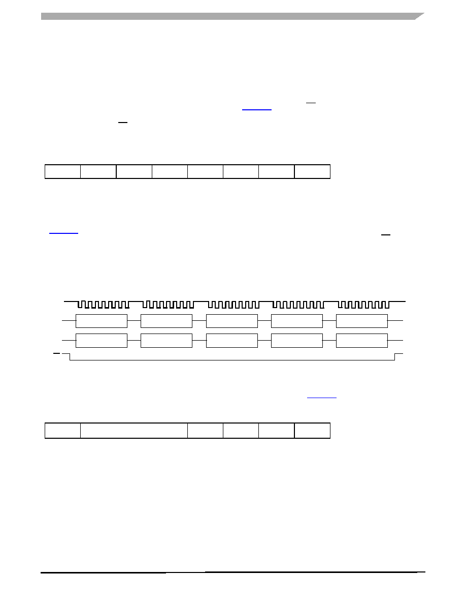
Figure 14 shows an example of a write operation. This
example assumes the last SPI transaction read or wrote the
data from register 00011 and is now pointing at 00100
(D01STAT). During the first byte of the SPI transaction, the
first MOSI bit is 1 (write) and the last five are 00000. During
this command byte, MISO returns the data from register
00100 (D01STAT). During the next SPI transactions, MOSI
updates the data in register 00000 with new data while
reading back the old data via MISO.
Although it looks like the read and write for an address are
occurring at the same time, the changes caused earlier
during the same burst would not be reflected by the data
returned, because the D01STAT is latched at CS going low.
When a short word is selected for Bus 0 (MS0 in D0CTRL
is set), the D0H register is skipped in the sequence. The
same is true for the D1H register when MS1 is set and
SWLEN1 = 1000.
Figure 14. SPI Burst Transfer Example
DBUS COMMUNICATIONS
The DBUS messages contain data from the DnH and DnL
registers. A CRC pattern is automatically appended to each
message. The data and CRC lengths are programmed by the
DnLENGTH register. Figure 15 shows the structure of the
DBUS message.
Figure 15. DBUS Communications Message
DBUS Driver/Receiver communications involve a frame
(DSIF), a data signal (DSIS), and a data return (DSIR) signal.
These are signals internal to the IC associated with the
protocol engine.
A message starts with a falling edge on the DSIF signal,
which marks the start of a frame. There is a one bit-time delay
before the MSB of data appears on the DSIS pin. Data bits
start with a falling edge on DSIS. The low time is 1/3 of the bit
time for a 1, and 2/3 of a bit time for a 0. Data is transmitted
on DSIS and received on DSIR pins simultaneously. Receive
data is the captured level on the DSIR pin at the end of each
bit time. At the end of the bit time for the last CRC bit, the
DSIF pin returns to a logic high (Idle level). A minimum delay
is imposed between successive frames as determined by the
DnCTRL register.
Users initiate a message by writing (via the SPI interface
from the MCU) to the low byte of the data register (DnL).
When 9- to 16-bit messages are to be sent, the user writes to
the DnH register first and then the DnL register before the
combined 9 to 16-bit data value DnH:DnL is sent on the
DBUS. The user should first check the TFNFn status flag to
be sure the transmit FIFO is not full before writing a new data
Bit 7
6
5
4
3
2
1
0
R/W
X
ADDR4
ADDR3
ADDR2
ADDR1
ADDR0
WR IT E CO MM AN D
P O IN T T O 00000
DA T A TO DS I0 H
( 00000)
D ATA TO DSI 0L
( 00001)
D ATA TO D SI 1H
(0 00 10 )
DA T A TO D SI1 L
(0 00 11 )
D ATA FR O M
D SI 01 ST A T( 00 10 0)
D ATA FR O M
D SI 0H ( 00 000 )
DA T A FR O M
D SI0 L (00001)
D ATA FRO M
DS I1H ( 0 001 0)
D ATA FR O M
D SI 1L ( 00 01 1)
CL K
MO S I
MI SO
CSB
WRITE COMMAND
POINT TO 00000
DATA FROM
D01STAT (00100)
DATA TO D0H
(00000)
DATA FROM D0H
(00000)
DATA TO D0L
(00001)
DATA FROM D0L
(00001)
DATA TO D1H
(00010)
DATA FROM D1H
(00010)
DATA TO D1L
(00011)
DATA FROM D1L
(00011)
CS
SCLK
Bit n
. . . . . . . . . . . . . . . .
Bit 0
CRC n
. . . . .
CRC 0
相关PDF资料 |
PDF描述 |
|---|---|
| MCZ33780EG | SPECIALTY MICROPROCESSOR CIRCUIT, PDSO16 |
| MC3S12Q64CFA8 | 16-BIT, FLASH, 8 MHz, MICROCONTROLLER, PQFP48 |
| MC3S12Q128VPB16 | 16-BIT, FLASH, 16 MHz, MICROCONTROLLER, PQFP52 |
| MC9S12Q32MPB16 | 16-BIT, FLASH, 16 MHz, MICROCONTROLLER, PQFP52 |
| MC3S12Q128CFA16 | 16-BIT, FLASH, 16 MHz, MICROCONTROLLER, PQFP48 |
相关代理商/技术参数 |
参数描述 |
|---|---|
| MC33790DW | 功能描述:IC DSI 2-CHAN INTERFACE 16-SOIC RoHS:否 类别:集成电路 (IC) >> 接口 - 传感器和探测器接口 系列:- 其它有关文件:Automotive Product Guide 产品培训模块:Lead (SnPb) Finish for COTS Obsolescence Mitigation Program 标准包装:74 系列:- 类型:触控式传感器 输入类型:数字 输出类型:数字 接口:JTAG,串行 电流 - 电源:100µA 安装类型:表面贴装 封装/外壳:20-TSSOP(0.173",4.40mm 宽) 供应商设备封装:20-TSSOP 包装:管件 |
| MC33790HEG | 功能描述:接口 - 专用 DISTRIB SYS INTRFC RoHS:否 制造商:Texas Instruments 产品类型:1080p60 Image Sensor Receiver 工作电源电压:1.8 V 电源电流:89 mA 最大功率耗散: 最大工作温度:+ 85 C 安装风格:SMD/SMT 封装 / 箱体:BGA-59 |
| MC33790HEGR2 | 功能描述:接口 - 专用 DISTRIB SYS INTRFC RoHS:否 制造商:Texas Instruments 产品类型:1080p60 Image Sensor Receiver 工作电源电压:1.8 V 电源电流:89 mA 最大功率耗散: 最大工作温度:+ 85 C 安装风格:SMD/SMT 封装 / 箱体:BGA-59 |
| MC33793D | 功能描述:IC DSI SLAVE FOR R-SENSE 16-SOIC RoHS:否 类别:集成电路 (IC) >> 接口 - 传感器和探测器接口 系列:- 其它有关文件:Automotive Product Guide 产品培训模块:Lead (SnPb) Finish for COTS Obsolescence Mitigation Program 标准包装:74 系列:- 类型:触控式传感器 输入类型:数字 输出类型:数字 接口:JTAG,串行 电流 - 电源:100µA 安装类型:表面贴装 封装/外壳:20-TSSOP(0.173",4.40mm 宽) 供应商设备封装:20-TSSOP 包装:管件 |
| MC33793DR2 | 功能描述:IC DSI SLAVE FOR R-SENSE 16-SOIC RoHS:否 类别:集成电路 (IC) >> 接口 - 传感器和探测器接口 系列:- 其它有关文件:Automotive Product Guide 产品培训模块:Lead (SnPb) Finish for COTS Obsolescence Mitigation Program 标准包装:74 系列:- 类型:触控式传感器 输入类型:数字 输出类型:数字 接口:JTAG,串行 电流 - 电源:100µA 安装类型:表面贴装 封装/外壳:20-TSSOP(0.173",4.40mm 宽) 供应商设备封装:20-TSSOP 包装:管件 |
发布紧急采购,3分钟左右您将得到回复。