- 您现在的位置:买卖IC网 > PDF目录67964 > MC56F8366VFVE (FREESCALE SEMICONDUCTOR INC) 16-BIT, 120 MHz, OTHER DSP, PQFP144 PDF资料下载
参数资料
| 型号: | MC56F8366VFVE |
| 厂商: | FREESCALE SEMICONDUCTOR INC |
| 元件分类: | 数字信号处理 |
| 英文描述: | 16-BIT, 120 MHz, OTHER DSP, PQFP144 |
| 封装: | ROHS COMPLIANT, LQFP-144 |
| 文件页数: | 100/182页 |
| 文件大小: | 1149K |
| 代理商: | MC56F8366VFVE |
第1页第2页第3页第4页第5页第6页第7页第8页第9页第10页第11页第12页第13页第14页第15页第16页第17页第18页第19页第20页第21页第22页第23页第24页第25页第26页第27页第28页第29页第30页第31页第32页第33页第34页第35页第36页第37页第38页第39页第40页第41页第42页第43页第44页第45页第46页第47页第48页第49页第50页第51页第52页第53页第54页第55页第56页第57页第58页第59页第60页第61页第62页第63页第64页第65页第66页第67页第68页第69页第70页第71页第72页第73页第74页第75页第76页第77页第78页第79页第80页第81页第82页第83页第84页第85页第86页第87页第88页第89页第90页第91页第92页第93页第94页第95页第96页第97页第98页第99页当前第100页第101页第102页第103页第104页第105页第106页第107页第108页第109页第110页第111页第112页第113页第114页第115页第116页第117页第118页第119页第120页第121页第122页第123页第124页第125页第126页第127页第128页第129页第130页第131页第132页第133页第134页第135页第136页第137页第138页第139页第140页第141页第142页第143页第144页第145页第146页第147页第148页第149页第150页第151页第152页第153页第154页第155页第156页第157页第158页第159页第160页第161页第162页第163页第164页第165页第166页第167页第168页第169页第170页第171页第172页第173页第174页第175页第176页第177页第178页第179页第180页第181页第182页
56F8366 Technical Data, Rev. 7
24
Freescale Semiconductor
Preliminary
RD
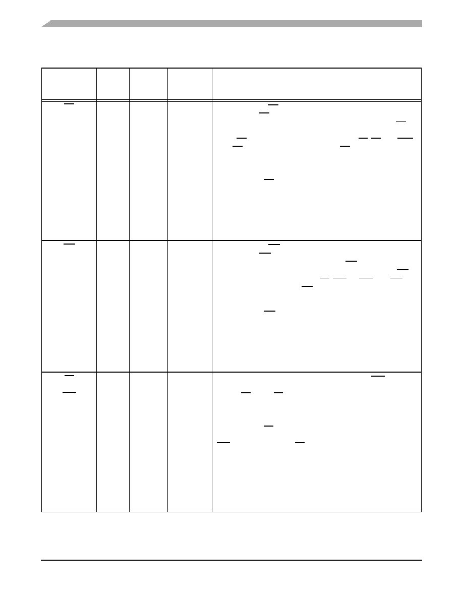
45
Output
In reset,
output is
disabled,
pull-up is
enabled
Read Enable — RD is asserted during external memory read
cycles. When RD is asserted low, pins D0 - D15 become inputs
and an external device is enabled onto the data bus. When RD is
deasserted high, the external data is latched inside the device.
When RD is asserted, it qualifies the A0 - A16, PS, DS, and CSn
pins. RD can be connected directly to the OE pin of a static RAM or
ROM.
Depending upon the state of the DRV bit in the EMI bus control
register (BCR), RD is tri-stated when the external bus is inactive.
Most designs will want to change the DRV state to DRV = 1 instead of
using the default setting.
To deactivate the internal pull-up resistor, set the CTRL bit in the
SIM_PUDR register.
WR
44
Output
In reset,
output is
disabled,
pull-up is
enabled
Write Enable — WR is asserted during external memory write
cycles. When WR is asserted low, pins D0 - D15 become outputs
and the device puts data on the bus. When WR is deasserted high,
the external data is latched inside the external device. When WR is
asserted, it qualifies the A0 - A16, PS, DS, and CSn pins. WR can
be connected directly to the WE pin of a static RAM.
Depending upon the state of the DRV bit in the EMI bus control
register (BCR), WR is tri-stated when the external bus is inactive.
Most designs will want to change the DRV state to DRV = 1 instead of
using the default setting.
To deactivate the internal pull-up resistor, set the CTRL bit in the
SIM_PUDR register.
PS
(CS0)
(GPIOD8)
46
Output
Input/
Output
In reset,
output is
disabled,
pull-up is
enabled
Program Memory Select — This signal is actually CS0 in the
EMI, which is programmed at reset for compatibility with the
56F80x PS signal. PS is asserted low for external program
memory access.
Depending upon the state of the DRV bit in the EMI bus control
register (BCR), PS is tri-stated when the external bus is inactive.
CS0 resets to provide the PS function as defined on the 56F80x
devices.
Port D GPIO — This GPIO pin can be individually programmed as
an input or output pin.
To deactivate the Internal pull-up resistor, clear bit 8 in the
GPIOD_PUR register.
Table 2-2 Signal and Package Information for the 144-Pin LQFP
Signal Name
Pin No.
Type
State
During
Reset
Signal Description
相关PDF资料 |
PDF描述 |
|---|---|
| MC56F8366VFV60 | 16-BIT, 120 MHz, OTHER DSP, PQFP144 |
| MC56F8335MFGE | 4-BIT, 120 MHz, OTHER DSP, PQFP128 |
| MC68008LC8 | 16-BIT, 8 MHz, MICROPROCESSOR, CDIP48 |
| MC68008L8 | 16-BIT, 8 MHz, MICROPROCESSOR, CDIP48 |
| MC68008CLC8 | 16-BIT, 8 MHz, MICROPROCESSOR, CDIP48 |
相关代理商/技术参数 |
参数描述 |
|---|---|
| MC56F8367 | 制造商:FREESCALE 制造商全称:Freescale Semiconductor, Inc 功能描述:16-bit Digital Signal Controllers |
| MC56F8367E | 制造商:FREESCALE 制造商全称:Freescale Semiconductor, Inc 功能描述:16-bit Digital Signal Controllers |
| MC56F8367EVM | 功能描述:开发板和工具包 - 其他处理器 MC56F8367 EVAL BOARD RoHS:否 制造商:Freescale Semiconductor 产品:Development Systems 工具用于评估:P3041 核心:e500mc 接口类型:I2C, SPI, USB 工作电源电压: |
| MC56F8367EVME | 功能描述:开发板和工具包 - 其他处理器 MC56F8367 EVALUATION BOARD RoHS:否 制造商:Freescale Semiconductor 产品:Development Systems 工具用于评估:P3041 核心:e500mc 接口类型:I2C, SPI, USB 工作电源电压: |
| MC56F8367EVME | 制造商:Freescale Semiconductor 功能描述:MC56F8367 EVALUATION BOA |
发布紧急采购,3分钟左右您将得到回复。