- 您现在的位置:买卖IC网 > PDF目录69027 > MC68HC08RC16DW (MOTOROLA INC) 8-BIT, MROM, MICROCONTROLLER, PDSO28 PDF资料下载
参数资料
| 型号: | MC68HC08RC16DW |
| 厂商: | MOTOROLA INC |
| 元件分类: | 微控制器/微处理器 |
| 英文描述: | 8-BIT, MROM, MICROCONTROLLER, PDSO28 |
| 封装: | SOIC-28 |
| 文件页数: | 103/200页 |
| 文件大小: | 1856K |
| 代理商: | MC68HC08RC16DW |
第1页第2页第3页第4页第5页第6页第7页第8页第9页第10页第11页第12页第13页第14页第15页第16页第17页第18页第19页第20页第21页第22页第23页第24页第25页第26页第27页第28页第29页第30页第31页第32页第33页第34页第35页第36页第37页第38页第39页第40页第41页第42页第43页第44页第45页第46页第47页第48页第49页第50页第51页第52页第53页第54页第55页第56页第57页第58页第59页第60页第61页第62页第63页第64页第65页第66页第67页第68页第69页第70页第71页第72页第73页第74页第75页第76页第77页第78页第79页第80页第81页第82页第83页第84页第85页第86页第87页第88页第89页第90页第91页第92页第93页第94页第95页第96页第97页第98页第99页第100页第101页第102页当前第103页第104页第105页第106页第107页第108页第109页第110页第111页第112页第113页第114页第115页第116页第117页第118页第119页第120页第121页第122页第123页第124页第125页第126页第127页第128页第129页第130页第131页第132页第133页第134页第135页第136页第137页第138页第139页第140页第141页第142页第143页第144页第145页第146页第147页第148页第149页第150页第151页第152页第153页第154页第155页第156页第157页第158页第159页第160页第161页第162页第163页第164页第165页第166页第167页第168页第169页第170页第171页第172页第173页第174页第175页第176页第177页第178页第179页第180页第181页第182页第183页第184页第185页第186页第187页第188页第189页第190页第191页第192页第193页第194页第195页第196页第197页第198页第199页第200页
Electrical Specifications
2.0-Volt DC Electrical Characteristics
MC68HC08RC16 — Rev. 1.0
Technical Data
MOTOROLA
Electrical Specifications
191
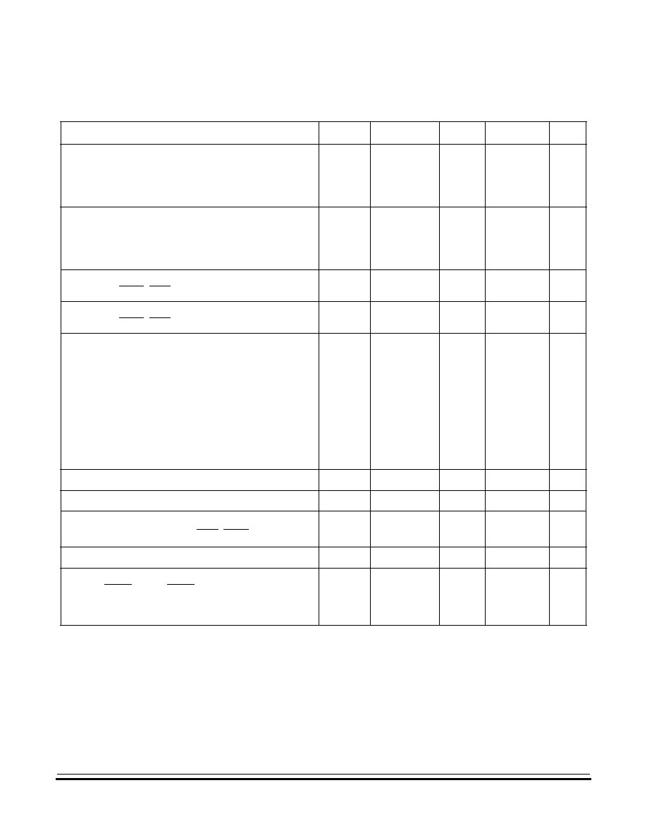
19.7 2.0-Volt DC Electrical Characteristics
Characteristic(1)
1. VDD = 2.0 Vdc ± 10%, VSS = 0 Vdc, TA = TL to TH, unless otherwise noted
Symbol
Min
Typ(2)
2. Typical values reflect average measurements at midpoint of voltage range, 25
°C only.
Max
Unit
Output high voltage
(ILoad = –1.2 mA) port A, port B
(ILoad = –6 mA) IRO
(ILoad = –1.2 mA) port C
VOH
VDD –0.3
VDD –0.7
VDD –0.3
—
V
Output low voltage
(ILoad = 2 mA) port A,port B
(ILoad = 11 mA) IRO
(ILoad = 7 mA) port C
VOL
—
0.3
0.8
0.3
V
Input high voltage
All ports, IRQ1, RST, BATT, OSC1
VIH
0.7 x VDD
—
VDD
V
Input low voltage
All ports, IRQ1, RST, BATT, OSC1
VIL
VSS
—
0.3 x VDD
V
VDD supply current
Run, fOP = 2.0 MHz
(3)
Wait (4)
Stop(5) or LP reset with battery in (6)
25
°C
0
°C to 70°C
LP reset with battery out (7)
25
°C
0
°C to 70°C
3. Run (operating) IDD measured using external square wave clock source. LVI enabled. All inputs 0.2 V from rail. No dc
loads. Less than 100 pF on all outputs. CL = 20 pF on OSC2. All ports configured as inputs. OSC2 capacitance linearly
affects run IDD. Measured with all modules enabled.
4. Wait IDD measured using external square wave clock source (fCGMXCLK = 4 MHz); all inputs 0.2 V from rail; no dc loads;
less than 100 pF on all outputs. CL = 20 pF on OSC2; OSC2 capacitance linearly affects wait IDD.
5. Stop IDD measured with OSC1 grounded and no port pins sourcing current. LVI is disabled by stop entry.
6. IDD measurement when BATT supply is below VLVR and part is in LP reset.
7. IDD measurement when BATT supply is removed and part is in LP reset.
IDD
—
1.0
0.5
0.3
0.1
1.0
0.6
0.3
0.1
mA
A
I/O ports hi-z leakage current
IIL
——
± 4
A
Input current
IIn
——
± 1
A
Capacitance
Ports (as input or output), RST, IRQ1, BATT
COut
CIn
—
12
8
pF
Monitor mode entry voltage
VTST
VDD + 2.5
—9
V
Pullup resistor
PTB7/KBD7–PTB0/KBD0
25
°C
0
°C to 70°C
RPU
27
24
—
39
48
k
相关PDF资料 |
PDF描述 |
|---|---|
| MC68HC11A8BVFU2 | 8-BIT, MROM, 2 MHz, MICROCONTROLLER, PQFP64 |
| MC68HC11A8BMFN2 | 8-BIT, MROM, 2 MHz, MICROCONTROLLER, PQCC52 |
| MC68HC11A8BVFN2 | 8-BIT, MROM, 2 MHz, MICROCONTROLLER, PQCC52 |
| MC68HC11D0CFB | 8-BIT, MICROCONTROLLER, PQFP44 |
| MC68HC11D0CP2 | 8-BIT, MROM, 2 MHz, MICROCONTROLLER, PDIP40 |
相关代理商/技术参数 |
参数描述 |
|---|---|
| MC68HC08SR12 | 制造商:FREESCALE 制造商全称:Freescale Semiconductor, Inc 功能描述:M68HC08 Microcontrollers |
| MC68HC08TV24CFB | 制造商:FREESCALE 制造商全称:Freescale Semiconductor, Inc 功能描述:M68HC08 Microcontrollers |
| MC68HC08XL36 | 制造商:FREESCALE 制造商全称:Freescale Semiconductor, Inc 功能描述:HCMOS Microcontroller Unit |
| MC68HC08XL36CB | 制造商:FREESCALE 制造商全称:Freescale Semiconductor, Inc 功能描述:HCMOS Microcontroller Unit |
| MC68HC08XL36CFU | 制造商:FREESCALE 制造商全称:Freescale Semiconductor, Inc 功能描述:HCMOS Microcontroller Unit |
发布紧急采购,3分钟左右您将得到回复。