- 您现在的位置:买卖IC网 > PDF目录80429 > MC908GR8MDWR2 (FREESCALE SEMICONDUCTOR INC) 8-BIT, FLASH, 8.2 MHz, MICROCONTROLLER, PDSO28 PDF资料下载
参数资料
| 型号: | MC908GR8MDWR2 |
| 厂商: | FREESCALE SEMICONDUCTOR INC |
| 元件分类: | 微控制器/微处理器 |
| 英文描述: | 8-BIT, FLASH, 8.2 MHz, MICROCONTROLLER, PDSO28 |
| 封装: | MS-013AE, SOIC-28 |
| 文件页数: | 188/286页 |
| 文件大小: | 3708K |
| 代理商: | MC908GR8MDWR2 |
第1页第2页第3页第4页第5页第6页第7页第8页第9页第10页第11页第12页第13页第14页第15页第16页第17页第18页第19页第20页第21页第22页第23页第24页第25页第26页第27页第28页第29页第30页第31页第32页第33页第34页第35页第36页第37页第38页第39页第40页第41页第42页第43页第44页第45页第46页第47页第48页第49页第50页第51页第52页第53页第54页第55页第56页第57页第58页第59页第60页第61页第62页第63页第64页第65页第66页第67页第68页第69页第70页第71页第72页第73页第74页第75页第76页第77页第78页第79页第80页第81页第82页第83页第84页第85页第86页第87页第88页第89页第90页第91页第92页第93页第94页第95页第96页第97页第98页第99页第100页第101页第102页第103页第104页第105页第106页第107页第108页第109页第110页第111页第112页第113页第114页第115页第116页第117页第118页第119页第120页第121页第122页第123页第124页第125页第126页第127页第128页第129页第130页第131页第132页第133页第134页第135页第136页第137页第138页第139页第140页第141页第142页第143页第144页第145页第146页第147页第148页第149页第150页第151页第152页第153页第154页第155页第156页第157页第158页第159页第160页第161页第162页第163页第164页第165页第166页第167页第168页第169页第170页第171页第172页第173页第174页第175页第176页第177页第178页第179页第180页第181页第182页第183页第184页第185页第186页第187页当前第188页第189页第190页第191页第192页第193页第194页第195页第196页第197页第198页第199页第200页第201页第202页第203页第204页第205页第206页第207页第208页第209页第210页第211页第212页第213页第214页第215页第216页第217页第218页第219页第220页第221页第222页第223页第224页第225页第226页第227页第228页第229页第230页第231页第232页第233页第234页第235页第236页第237页第238页第239页第240页第241页第242页第243页第244页第245页第246页第247页第248页第249页第250页第251页第252页第253页第254页第255页第256页第257页第258页第259页第260页第261页第262页第263页第264页第265页第266页第267页第268页第269页第270页第271页第272页第273页第274页第275页第276页第277页第278页第279页第280页第281页第282页第283页第284页第285页第286页
Electrical Specifications
MC68HC908GR8 MC68HC908GR4 Data Sheet, Rev. 7
268
Freescale Semiconductor
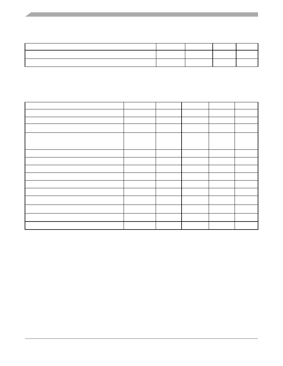
23.15 Timer Interface Module Characteristics
23.16 Memory Characteristics
Characteristic
Symbol
Min
Max
Unit
Input capture pulse width
tTIH, tTIL
2—
tcyc
Timer input capture period
tTLTL
See Note(1)
1. The minimum period is the number of cycles it takes to execute the interrupt service routine plus 1 tcyc.
—
tcyc
Characteristic
Symbol
Min
Typ
Max
Unit
RAM data retention voltage
VRDR
1.3
—
V
FLASH program bus clock frequency
—
1
—
MHz
FLASH read bus clock frequency
fRead
(1)
1. fRead is defined as the frequency range for which the FLASH memory can be read.
32k
—
8.4M
Hz
FLASH page erase time
Limited endurance (<1 K cycles)
Maximum endurance (> 1 K cycles)
tErase
0.9
3.6
1
4
1.1
5.5
ms
FLASH mass erase time
tMErase
4—
—
ms
FLASH PGM/ERASE to HVEN set up time
tnvs
10
—
μs
FLASH high-voltage hold time
tnvh
5—
—
μs
FLASH high-voltage hold time (mass erase)
tnvhl
100
—
μs
FLASH program hold time
tpgs
5—
—
μs
FLASH program time
tPROG
30
—
40
μs
FLASH return to read time
trcv
(2)
2. trcv is defined as the time it needs before the FLASH can be read after turning off the high voltage charge pump, by clearing
HVEN to 0.
1—
—
μs
FLASH cumulative program HV period
tHV
(3)
3. tHV is defined as the cumulative high voltage programming time to the same row before next erase.
tHV must satisfy this condition: tnvs + tnvh + tpgs + (tPROG × 64) ≤ tHV max.
——
4
ms
FLASH endurance(4)
4. Typical endurance was evaluated for this product family. For additional information on how Freescale defines typical
Endurance, please refer to Engineering Bulletin EB619.
—
10k
100k
—
Cycles
FLASH data retention time(5)
5. Typical data retention values are based on intrinsic capability of the technology measured at high temperature and de-rated
to 25°C using the Arrhenius equation. For additional information on how Freescale defines Typical Data Retention, please
refer to Engineering Bulletin EB618.
—
15
100
—
Years
相关PDF资料 |
PDF描述 |
|---|---|
| MC9S08RC8CFG | 8-BIT, FLASH, 8 MHz, MICROCONTROLLER, PQFP44 |
| MC9S08RD16CDWE | 8-BIT, FLASH, 8 MHz, MICROCONTROLLER, PDSO28 |
| MC9S08RD32FJ | 8-BIT, FLASH, 8 MHz, MICROCONTROLLER, PQFP32 |
| MC68HC11E20CFU3 | 8-BIT, MROM, 3 MHz, MICROCONTROLLER, PQFP64 |
| MC68HC908QT4VFQ | 8-BIT, FLASH, 8 MHz, MICROCONTROLLER, DSO8 |
相关代理商/技术参数 |
参数描述 |
|---|---|
| MC908GR8MFAR2 | 制造商:FREESCALE 制造商全称:Freescale Semiconductor, Inc 功能描述:M68HC08 Microcontrollers |
| MC908GR8VDWR2 | 制造商:MOTOROLA 制造商全称:Motorola, Inc 功能描述:Microcontrollers |
| MC908GR8VFAR2 | 制造商:MOTOROLA 制造商全称:Motorola, Inc 功能描述:Microcontrollers |
| MC908GT16 | 制造商:FREESCALE 制造商全称:Freescale Semiconductor, Inc 功能描述:MC908GT16 |
| MC908GT16CB | 制造商:FREESCALE 制造商全称:Freescale Semiconductor, Inc 功能描述:Microcontrollers |
发布紧急采购,3分钟左右您将得到回复。