- 您现在的位置:买卖IC网 > PDF目录80429 > MC908GR8MDWR2 (FREESCALE SEMICONDUCTOR INC) 8-BIT, FLASH, 8.2 MHz, MICROCONTROLLER, PDSO28 PDF资料下载
参数资料
| 型号: | MC908GR8MDWR2 |
| 厂商: | FREESCALE SEMICONDUCTOR INC |
| 元件分类: | 微控制器/微处理器 |
| 英文描述: | 8-BIT, FLASH, 8.2 MHz, MICROCONTROLLER, PDSO28 |
| 封装: | MS-013AE, SOIC-28 |
| 文件页数: | 40/286页 |
| 文件大小: | 3708K |
| 代理商: | MC908GR8MDWR2 |
第1页第2页第3页第4页第5页第6页第7页第8页第9页第10页第11页第12页第13页第14页第15页第16页第17页第18页第19页第20页第21页第22页第23页第24页第25页第26页第27页第28页第29页第30页第31页第32页第33页第34页第35页第36页第37页第38页第39页当前第40页第41页第42页第43页第44页第45页第46页第47页第48页第49页第50页第51页第52页第53页第54页第55页第56页第57页第58页第59页第60页第61页第62页第63页第64页第65页第66页第67页第68页第69页第70页第71页第72页第73页第74页第75页第76页第77页第78页第79页第80页第81页第82页第83页第84页第85页第86页第87页第88页第89页第90页第91页第92页第93页第94页第95页第96页第97页第98页第99页第100页第101页第102页第103页第104页第105页第106页第107页第108页第109页第110页第111页第112页第113页第114页第115页第116页第117页第118页第119页第120页第121页第122页第123页第124页第125页第126页第127页第128页第129页第130页第131页第132页第133页第134页第135页第136页第137页第138页第139页第140页第141页第142页第143页第144页第145页第146页第147页第148页第149页第150页第151页第152页第153页第154页第155页第156页第157页第158页第159页第160页第161页第162页第163页第164页第165页第166页第167页第168页第169页第170页第171页第172页第173页第174页第175页第176页第177页第178页第179页第180页第181页第182页第183页第184页第185页第186页第187页第188页第189页第190页第191页第192页第193页第194页第195页第196页第197页第198页第199页第200页第201页第202页第203页第204页第205页第206页第207页第208页第209页第210页第211页第212页第213页第214页第215页第216页第217页第218页第219页第220页第221页第222页第223页第224页第225页第226页第227页第228页第229页第230页第231页第232页第233页第234页第235页第236页第237页第238页第239页第240页第241页第242页第243页第244页第245页第246页第247页第248页第249页第250页第251页第252页第253页第254页第255页第256页第257页第258页第259页第260页第261页第262页第263页第264页第265页第266页第267页第268页第269页第270页第271页第272页第273页第274页第275页第276页第277页第278页第279页第280页第281页第282页第283页第284页第285页第286页
Monitor ROM (MON)
MC68HC908GR8 MC68HC908GR4 Data Sheet, Rev. 7
134
Freescale Semiconductor
Figure 15-2 shows a simplified diagram of the monitor mode entry when the reset vector is blank and just
1 x VDD voltage is applied to the IRQ pin. An external oscillator of 9.8304 MHz is required for a baud rate
of 9600, as the internal bus frequency is automatically set to the external frequency divided by four.
Enter monitor mode with pin configuration shown in Figure 15-1 by pulling RST low and then high. The
rising edge of RST latches monitor mode. Once monitor mode is latched, the values on the specified pins
can change.
Once out of reset, the MCU waits for the host to send eight security bytes. (See Security.) After the
security bytes, the MCU sends a break signal (10 consecutive logic 0s) to the host, indicating that it is
ready to receive a command.
NOTE
The PTA1 pin must remain at logic 0 for 24 bus cycles after the RST pin
goes high to enter monitor mode properly.
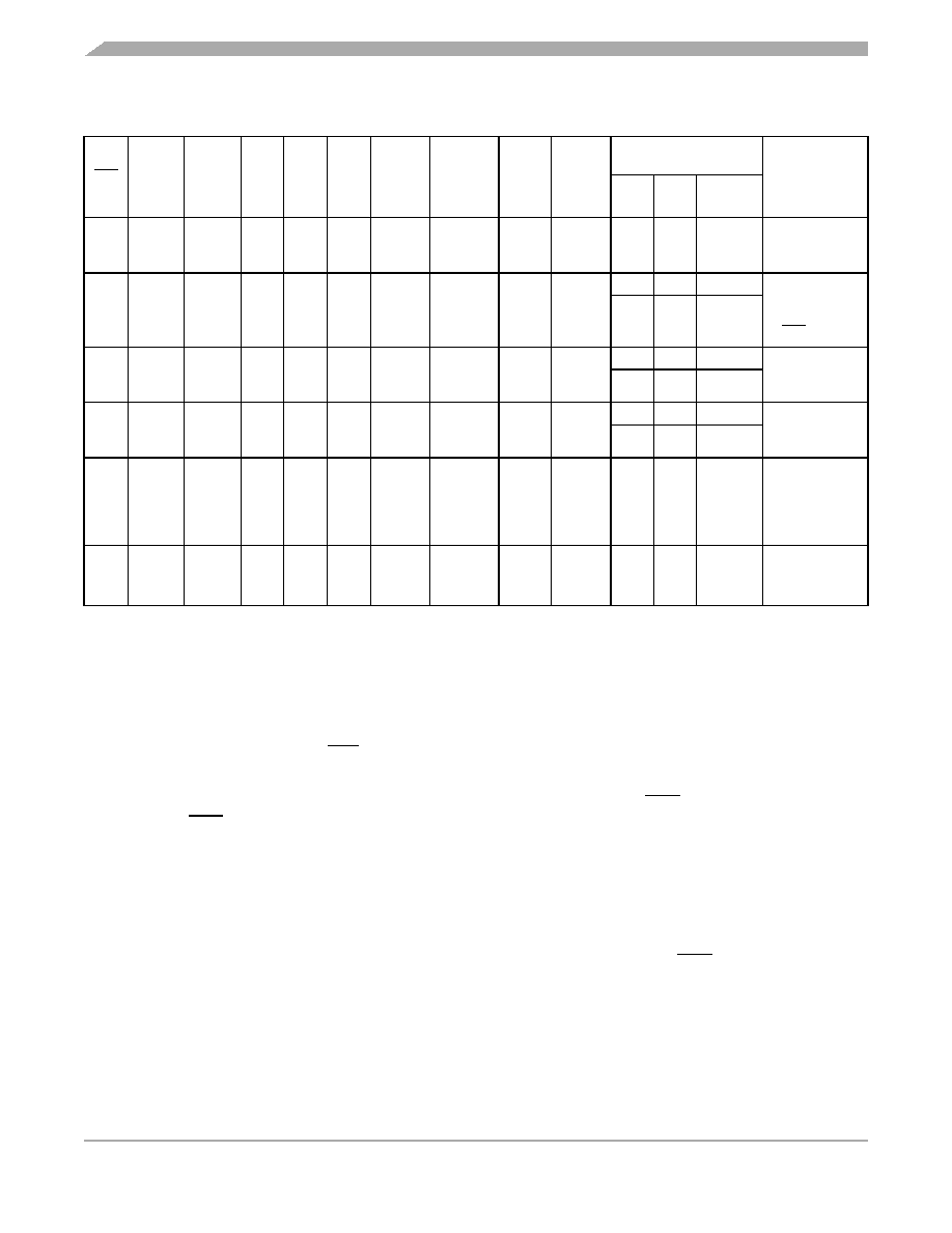
Table 15-1. Monitor Mode Signal Requirements and Options
IRQ
RESET
$FFFE/
$FFFF
PLL
PTB0 PTB1
External
Clock(1)
1. External clock is derived by a 32.768 kHz crystal or a 9.8304 MHz off-chip oscillator
CGMOUT
Bus
Freq
COP
For Serial
Communication
Comment
PTA0 PTA1
Baud
Rate(2) (3)
2. PTA0 = 1 if serial communication; PTA0 = X if parallel communication
3. PTA1 = 0
→ serial, PTA1 = 1 → parallel communication for security code entry
4. DNA = does not apply, X = don’t care
XGND
X
0
Disabled
X
0
No operation
until reset goes
high
VTST
VDD
or
VTST
XOFF
1
0
9.8304
MHz
4.9152
MHz
2.4576
MHz
Disabled
1
0
9600
PTB0 and PTB1
voltages only
required if
IRQ =VTST
X1
DNA
VDD
$FFFF
OFF
X
9.8304
MHz
4.9152
MHz
2.4576
MHz
Disabled
1
0
9600
External
frequency always
divided by 4
X1
DNA
GND
VDD
$FFFF
ON
X
32.768
kHz
4.9152
MHz
2.4576
MHz
Disabled
1
0
9600
PLL enabled
(BCS set) in
monitor code
X1
DNA
VDD
or
GND
VTST
$FFFF
OFF
X
—
Enabled
X
—
Enters user
mode — will
encounter an
illegal address
reset
VDD
or
GND
VDD
or
VTST
Not
$FFFF
OFF
X
—
Enabled
X
—
Enters
user mode
相关PDF资料 |
PDF描述 |
|---|---|
| MC9S08RC8CFG | 8-BIT, FLASH, 8 MHz, MICROCONTROLLER, PQFP44 |
| MC9S08RD16CDWE | 8-BIT, FLASH, 8 MHz, MICROCONTROLLER, PDSO28 |
| MC9S08RD32FJ | 8-BIT, FLASH, 8 MHz, MICROCONTROLLER, PQFP32 |
| MC68HC11E20CFU3 | 8-BIT, MROM, 3 MHz, MICROCONTROLLER, PQFP64 |
| MC68HC908QT4VFQ | 8-BIT, FLASH, 8 MHz, MICROCONTROLLER, DSO8 |
相关代理商/技术参数 |
参数描述 |
|---|---|
| MC908GR8MFAR2 | 制造商:FREESCALE 制造商全称:Freescale Semiconductor, Inc 功能描述:M68HC08 Microcontrollers |
| MC908GR8VDWR2 | 制造商:MOTOROLA 制造商全称:Motorola, Inc 功能描述:Microcontrollers |
| MC908GR8VFAR2 | 制造商:MOTOROLA 制造商全称:Motorola, Inc 功能描述:Microcontrollers |
| MC908GT16 | 制造商:FREESCALE 制造商全称:Freescale Semiconductor, Inc 功能描述:MC908GT16 |
| MC908GT16CB | 制造商:FREESCALE 制造商全称:Freescale Semiconductor, Inc 功能描述:Microcontrollers |
发布紧急采购,3分钟左右您将得到回复。