- 您现在的位置:买卖IC网 > PDF目录80429 > MC908GR8MDWR2 (FREESCALE SEMICONDUCTOR INC) 8-BIT, FLASH, 8.2 MHz, MICROCONTROLLER, PDSO28 PDF资料下载
参数资料
| 型号: | MC908GR8MDWR2 |
| 厂商: | FREESCALE SEMICONDUCTOR INC |
| 元件分类: | 微控制器/微处理器 |
| 英文描述: | 8-BIT, FLASH, 8.2 MHz, MICROCONTROLLER, PDSO28 |
| 封装: | MS-013AE, SOIC-28 |
| 文件页数: | 78/286页 |
| 文件大小: | 3708K |
| 代理商: | MC908GR8MDWR2 |
第1页第2页第3页第4页第5页第6页第7页第8页第9页第10页第11页第12页第13页第14页第15页第16页第17页第18页第19页第20页第21页第22页第23页第24页第25页第26页第27页第28页第29页第30页第31页第32页第33页第34页第35页第36页第37页第38页第39页第40页第41页第42页第43页第44页第45页第46页第47页第48页第49页第50页第51页第52页第53页第54页第55页第56页第57页第58页第59页第60页第61页第62页第63页第64页第65页第66页第67页第68页第69页第70页第71页第72页第73页第74页第75页第76页第77页当前第78页第79页第80页第81页第82页第83页第84页第85页第86页第87页第88页第89页第90页第91页第92页第93页第94页第95页第96页第97页第98页第99页第100页第101页第102页第103页第104页第105页第106页第107页第108页第109页第110页第111页第112页第113页第114页第115页第116页第117页第118页第119页第120页第121页第122页第123页第124页第125页第126页第127页第128页第129页第130页第131页第132页第133页第134页第135页第136页第137页第138页第139页第140页第141页第142页第143页第144页第145页第146页第147页第148页第149页第150页第151页第152页第153页第154页第155页第156页第157页第158页第159页第160页第161页第162页第163页第164页第165页第166页第167页第168页第169页第170页第171页第172页第173页第174页第175页第176页第177页第178页第179页第180页第181页第182页第183页第184页第185页第186页第187页第188页第189页第190页第191页第192页第193页第194页第195页第196页第197页第198页第199页第200页第201页第202页第203页第204页第205页第206页第207页第208页第209页第210页第211页第212页第213页第214页第215页第216页第217页第218页第219页第220页第221页第222页第223页第224页第225页第226页第227页第228页第229页第230页第231页第232页第233页第234页第235页第236页第237页第238页第239页第240页第241页第242页第243页第244页第245页第246页第247页第248页第249页第250页第251页第252页第253页第254页第255页第256页第257页第258页第259页第260页第261页第262页第263页第264页第265页第266页第267页第268页第269页第270页第271页第272页第273页第274页第275页第276页第277页第278页第279页第280页第281页第282页第283页第284页第285页第286页
Functional Description
MC68HC908GR8 MC68HC908GR4 Data Sheet, Rev. 7
Freescale Semiconductor
169
18.4.3.2 Character Reception
During an SCI reception, the receive shift register shifts characters in from the PE1/RxD pin. The SCI data
register (SCDR) is the read-only buffer between the internal data bus and the receive shift register.
After a complete character shifts into the receive shift register, the data portion of the character transfers
to the SCDR. The SCI receiver full bit, SCRF, in SCI status register 1 (SCS1) becomes set, indicating that
the received byte can be read. If the SCI receive interrupt enable bit, SCRIE, in SCC2 is also set, the
SCRF bit generates a receiver CPU interrupt request.
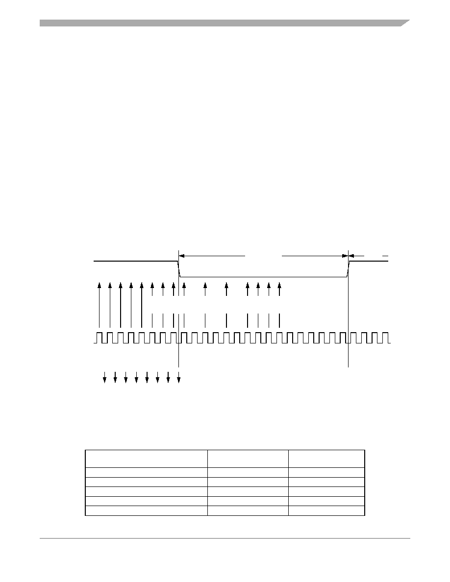
18.4.3.3 Data Sampling
The receiver samples the PE1/RxD pin at the RT clock rate. The RT clock is an internal signal with a
frequency 16 times the baud rate. To adjust for baud rate mismatch, the RT clock is resynchronized at
the following times (see Figure 18-6):
After every start bit
After the receiver detects a data bit change from 1 to 0 (after the majority of data bit samples at
RT8, RT9, and RT10 returns a valid 1 and the majority of the next RT8, RT9, and RT10 samples
returns a valid 0)
To locate the start bit, data recovery does an asynchronous search for a 0 preceded by three 1s. When
the falling edge of a possible start bit occurs, the RT clock begins to count to 16.
Figure 18-6. Receiver Data Sampling
To verify the start bit and to detect noise, data recovery logic takes samples at RT3, RT5, and RT7.
Table 18-2 summarizes the results of the start bit verification samples.
Table 18-2. Start Bit Verification
RT3, RT5, and RT7 Samples
Start Bit
Verification
Noise Flag
000
Yes
0
001
Yes
1
010
Yes
1
011
No
0
100
Yes
1
RT CLOCK
RESET
RT
1
RT
1
RT
1
RT
1
RT
1
RT
1
RT
1
RT
1
RT
1
RT
2
RT
3
RT
4
RT
5
RT
8
RT
7
RT
6
R
T11
R
T10
RT
9
R
T15
R
T14
R
T13
R
T12
R
T16
RT
1
RT
2
RT
3
RT
4
START BIT
QUALIFICATION
START BIT
VERIFICATION
DATA
SAMPLING
SAMPLES
RT
CLOCK
RT CLOCK
STATE
START BIT
LSB
PE1/RxD
相关PDF资料 |
PDF描述 |
|---|---|
| MC9S08RC8CFG | 8-BIT, FLASH, 8 MHz, MICROCONTROLLER, PQFP44 |
| MC9S08RD16CDWE | 8-BIT, FLASH, 8 MHz, MICROCONTROLLER, PDSO28 |
| MC9S08RD32FJ | 8-BIT, FLASH, 8 MHz, MICROCONTROLLER, PQFP32 |
| MC68HC11E20CFU3 | 8-BIT, MROM, 3 MHz, MICROCONTROLLER, PQFP64 |
| MC68HC908QT4VFQ | 8-BIT, FLASH, 8 MHz, MICROCONTROLLER, DSO8 |
相关代理商/技术参数 |
参数描述 |
|---|---|
| MC908GR8MFAR2 | 制造商:FREESCALE 制造商全称:Freescale Semiconductor, Inc 功能描述:M68HC08 Microcontrollers |
| MC908GR8VDWR2 | 制造商:MOTOROLA 制造商全称:Motorola, Inc 功能描述:Microcontrollers |
| MC908GR8VFAR2 | 制造商:MOTOROLA 制造商全称:Motorola, Inc 功能描述:Microcontrollers |
| MC908GT16 | 制造商:FREESCALE 制造商全称:Freescale Semiconductor, Inc 功能描述:MC908GT16 |
| MC908GT16CB | 制造商:FREESCALE 制造商全称:Freescale Semiconductor, Inc 功能描述:Microcontrollers |
发布紧急采购,3分钟左右您将得到回复。