- 您现在的位置:买卖IC网 > PDF目录69030 > MC9328MXSCVF10 (FREESCALE SEMICONDUCTOR INC) 32-BIT, 100 MHz, MICROPROCESSOR, PBGA225 PDF资料下载
参数资料
| 型号: | MC9328MXSCVF10 |
| 厂商: | FREESCALE SEMICONDUCTOR INC |
| 元件分类: | 微控制器/微处理器 |
| 英文描述: | 32-BIT, 100 MHz, MICROPROCESSOR, PBGA225 |
| 封装: | 13 X 13 MM, PLASTIC, BGA-225 |
| 文件页数: | 65/72页 |
| 文件大小: | 1411K |
| 代理商: | MC9328MXSCVF10 |
第1页第2页第3页第4页第5页第6页第7页第8页第9页第10页第11页第12页第13页第14页第15页第16页第17页第18页第19页第20页第21页第22页第23页第24页第25页第26页第27页第28页第29页第30页第31页第32页第33页第34页第35页第36页第37页第38页第39页第40页第41页第42页第43页第44页第45页第46页第47页第48页第49页第50页第51页第52页第53页第54页第55页第56页第57页第58页第59页第60页第61页第62页第63页第64页当前第65页第66页第67页第68页第69页第70页第71页第72页
MC9328MXS Advance Information, Rev. 0
68
Freescale Semiconductor
Specifications
16
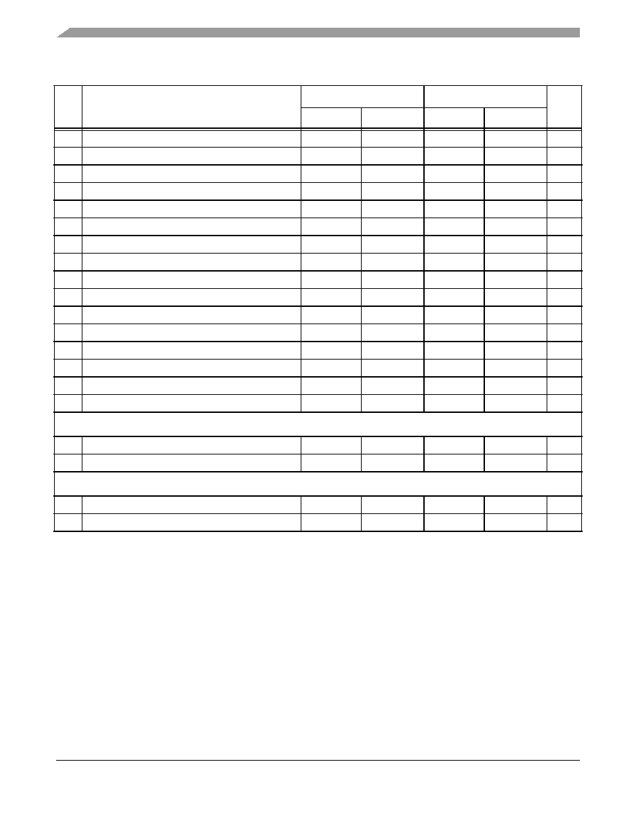
STCK/SRCK clock high period
27.1
–
40.7
–
ns
17
STCK/SRCK clock low period
61.1
–
40.7
–
ns
18
STCK high to STFS (bl) high3
–
92.8
0
81.4
ns
19
SRCK high to SRFS (bl) high3
–
92.8
0
81.4
ns
20
STCK high to STFS (bl) low3
–
92.8
0
81.4
ns
21
SRCK high to SRFS (bl) low3
–
92.8
0
81.4
ns
22
STCK high to STFS (wl) high3
–
92.8
0
81.4
ns
23
SRCK high to SRFS (wl) high3
–
92.8
0
81.4
ns
24
STCK high to STFS (wl) low3
–
92.8
0
81.4
ns
25
SRCK high to SRFS (wl) low3
–
92.8
0
81.4
ns
26
STCK high to STXD valid from high impedance
18.9
29.07
16.6
25.5
ns
27a
STCK high to STXD high
9.23
20.75
8.1
18.2
ns
27b
STCK high to STXD low
10.60
21.32
9.3
18.7
ns
28
STCK high to STXD high impedance
17.90
29.75
15.7
26.1
ns
29
SRXD setup time before SRCK low
1.14
–
1.0
–
ns
30
SRXD hold time after SRCK low
0
–
0
–
ns
Synchronous Internal Clock Operation (Port B Alternate Function2)
31
SRXD setup before STCK falling
18.81
–
16.5
–
ns
32
SRXD hold after STCK falling
0
–
0
–
ns
Synchronous External Clock Operation (Port B Alternate Function2)
33
SRXD setup before STCK falling
1.14
–
1.0
–
ns
34
SRXD hold after STCK falling
0
–
0
–
ns
1.
All the timings for the SSI are given for a non-inverted serial clock polarity (TSCKP/RSCKP = 0) and a non-inverted
frame sync (TFSI/RFSI = 0). If the polarity of the clock and/or the frame sync have been inverted, all the timing
remains valid by inverting the clock signal STCK/SRCK and/or the frame sync STFS/SRFS shown in the tables and
in the figures.
2.
There are 2 set of I/O signals for the SSI module. They are from Port C primary function (pad 257 to pad 261) and
Port B alternate function (pad 283 to pad 288). When SSI signals are configured as outputs, they can be viewed
both at Port C primary function and Port B alternate function. When SSI signals are configured as inputs, the SSI
module selects the input based on FMCR register bits in the Clock controller module (CRM). By default, the input
are selected from Port C primary function.
3.
bl = bit length; wl = word length.
Table 33. SSI (Port B Alternate Function) Timing Parameter Table (Continued)
Ref
No.
Parameter
1.8 ± 0.1 V
3.0 ± 0.3 V
Unit
Minimum
Maximum
Minimum
Maximum
相关PDF资料 |
PDF描述 |
|---|---|
| MC9328MXSCVP10R2 | 32-BIT, 100 MHz, MICROPROCESSOR, PBGA225 |
| MC94MX21DVKN3R2 | 350 MHz, MICROPROCESSOR, PBGA289 |
| MC9S08FL8CLC | 8-BIT, FLASH, 20 MHz, MICROCONTROLLER, QFP32 |
| MC9S08FL8CBM | 8-BIT, FLASH, 20 MHz, MICROCONTROLLER, PDIP32 |
| MC9S08FL16CBM | 8-BIT, FLASH, 20 MHz, MICROCONTROLLER, PDIP32 |
相关代理商/技术参数 |
参数描述 |
|---|---|
| MC9328MXSCVF10(R2) | 制造商:未知厂家 制造商全称:未知厂家 功能描述:Advance Information |
| MC9328MXSCVF10R2 | 制造商:未知厂家 制造商全称:未知厂家 功能描述:Advance Information |
| MC9328MXSCVP10 | 功能描述:处理器 - 专门应用 REDUCED FEATURE I.MXL RoHS:否 制造商:Freescale Semiconductor 类型:Multimedia Applications 核心:ARM Cortex A9 处理器系列:i.MX6 数据总线宽度:32 bit 最大时钟频率:1 GHz 指令/数据缓存: 数据 RAM 大小:128 KB 数据 ROM 大小: 工作电源电压: 最大工作温度:+ 95 C 安装风格:SMD/SMT 封装 / 箱体:MAPBGA-432 |
| MC9328MXSCVP10R2 | 功能描述:处理器 - 专门应用 REDUCED FEATURE I.MXL RoHS:否 制造商:Freescale Semiconductor 类型:Multimedia Applications 核心:ARM Cortex A9 处理器系列:i.MX6 数据总线宽度:32 bit 最大时钟频率:1 GHz 指令/数据缓存: 数据 RAM 大小:128 KB 数据 ROM 大小: 工作电源电压: 最大工作温度:+ 95 C 安装风格:SMD/SMT 封装 / 箱体:MAPBGA-432 |
| MC9328MXSVP10 | 功能描述:处理器 - 专门应用 REDUCED FEATURE CORSICA RoHS:否 制造商:Freescale Semiconductor 类型:Multimedia Applications 核心:ARM Cortex A9 处理器系列:i.MX6 数据总线宽度:32 bit 最大时钟频率:1 GHz 指令/数据缓存: 数据 RAM 大小:128 KB 数据 ROM 大小: 工作电源电压: 最大工作温度:+ 95 C 安装风格:SMD/SMT 封装 / 箱体:MAPBGA-432 |
发布紧急采购,3分钟左右您将得到回复。