- 您现在的位置:买卖IC网 > PDF目录11663 > MC9RS08KA2CDB (Freescale Semiconductor)IC MCU 8-BIT 2K FLASH 6-DFN PDF资料下载
参数资料
| 型号: | MC9RS08KA2CDB |
| 厂商: | Freescale Semiconductor |
| 文件页数: | 78/136页 |
| 文件大小: | 0K |
| 描述: | IC MCU 8-BIT 2K FLASH 6-DFN |
| 产品培训模块: | Mechatronics USBSpyder08 Discovery Kit RS08KA2 Low-End Microcontroller Series MC9RS08KA8 Microcontroller |
| 标准包装: | 490 |
| 系列: | RS08 |
| 核心处理器: | RS08 |
| 芯体尺寸: | 8-位 |
| 速度: | 10MHz |
| 外围设备: | LVD,POR,WDT |
| 输入/输出数: | 2 |
| 程序存储器容量: | 2KB(2K x 8) |
| 程序存储器类型: | 闪存 |
| RAM 容量: | 63 x 8 |
| 电压 - 电源 (Vcc/Vdd): | 1.8 V ~ 5.5 V |
| 振荡器型: | 内部 |
| 工作温度: | -40°C ~ 85°C |
| 封装/外壳: | 6-VDFN 裸露焊盘 |
| 包装: | 托盘 |
| 产品目录页面: | 726 (CN2011-ZH PDF) |
| 配用: | DEMO9RS08KA2-ND - DEMO BOARD FOR 9RS08KA2 |
第1页第2页第3页第4页第5页第6页第7页第8页第9页第10页第11页第12页第13页第14页第15页第16页第17页第18页第19页第20页第21页第22页第23页第24页第25页第26页第27页第28页第29页第30页第31页第32页第33页第34页第35页第36页第37页第38页第39页第40页第41页第42页第43页第44页第45页第46页第47页第48页第49页第50页第51页第52页第53页第54页第55页第56页第57页第58页第59页第60页第61页第62页第63页第64页第65页第66页第67页第68页第69页第70页第71页第72页第73页第74页第75页第76页第77页当前第78页第79页第80页第81页第82页第83页第84页第85页第86页第87页第88页第89页第90页第91页第92页第93页第94页第95页第96页第97页第98页第99页第100页第101页第102页第103页第104页第105页第106页第107页第108页第109页第110页第111页第112页第113页第114页第115页第116页第117页第118页第119页第120页第121页第122页第123页第124页第125页第126页第127页第128页第129页第130页第131页第132页第133页第134页第135页第136页
Chapter 6 Parallel Input/Output Control
MC9RS08KA2 Series Data Sheet, Rev. 4
46
Freescale Semiconductor
When a shared digital function is enabled for a pin, the output buffer is controlled by the shared function.
However, the data direction register bit will continue to control the source for reads of the port data register.
When a shared analog function is enabled for a pin, both the input and output buffers are disabled. A value
of 0 is read for any port data bit where the bit is an input (PTADDn = 0) and the input buffer is disabled.
In general, whenever a pin is shared with both an alternative digital function and an analog function, the
analog function has priority such that if both the digital and analog functions are enabled, the analog
function controls the pin.
It is a good programming practice to write to the port data register before changing the direction of a port
pin to become an output. This ensures that the pin will not be driven temporarily with an old data value
that happened to be in the port data register.
Associated with the parallel I/O ports is a set of registers located in the high page register space that operate
independently of the parallel I/O registers. These registers are used to control pullup/pulldown and slew
rate for the pins. See Section 6.3, “Pin Control Registers” for more information.
6.1
Pin Behavior in Low-Power Modes
In wait and stop modes, all pin states are maintained because internal logic stays powered up. Upon
recovery, all pin functions are the same as before entering stop.
6.2
Parallel I/O Registers
This section provides information about the registers associated with the parallel I/O ports. The parallel
I/O registers are located within the $001F memory boundary of the memory map, so that short and direct
addressing mode instructions can be used.
Refer to tables in Chapter 4, “Memory,” for the absolute address assignments for all parallel I/O. This
section refers to registers and control bits only by their names. A Freescale Semiconductor-provided
equate or header file normally is used to translate these names into the appropriate absolute addresses.
6.2.1
Port A Registers
Port A parallel I/O function is controlled by the data and data direction registers described in this section.
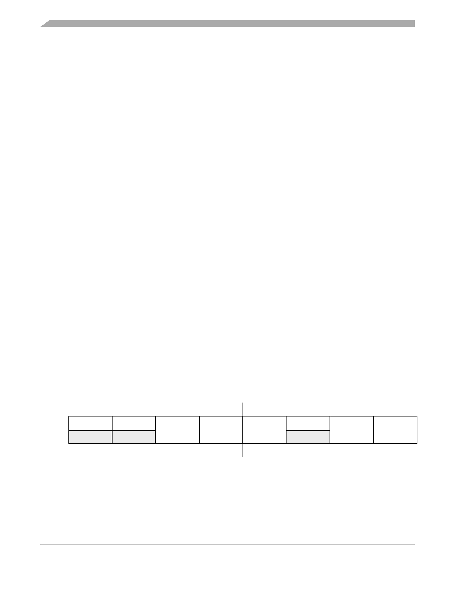
76
54
321
0
R
00
PTAD2
W
Reset:
000
00
000
Figure 6-2. Port A Data Register (PTAD)
相关PDF资料 |
PDF描述 |
|---|---|
| RE46C107S16F | IC HORN DRIVER DUAL 16SOIC |
| RE46C117E8F | IC HORN DRIVER DUAL 8PDIP |
| MC9S08SF4MTJ | MCU 8BIT 4K FLASH 20-TSSOP |
| MC9S08QE4CWJ | IC MCU 8BIT 4K FLASH 20-SOIC |
| MC9S08SH4CWJ | MCU 8BIT 4K FLASH 20-SOIC |
相关代理商/技术参数 |
参数描述 |
|---|---|
| MC9RS08KA2CPC | 功能描述:8位微控制器 -MCU 2K FLASH W/ ACMP 62 RAM RoHS:否 制造商:Silicon Labs 核心:8051 处理器系列:C8051F39x 数据总线宽度:8 bit 最大时钟频率:50 MHz 程序存储器大小:16 KB 数据 RAM 大小:1 KB 片上 ADC:Yes 工作电源电压:1.8 V to 3.6 V 工作温度范围:- 40 C to + 105 C 封装 / 箱体:QFN-20 安装风格:SMD/SMT |
| MC9RS08KA2CSC | 功能描述:8位微控制器 -MCU 2K FLASH W/ ACMP 62 RAM RoHS:否 制造商:Silicon Labs 核心:8051 处理器系列:C8051F39x 数据总线宽度:8 bit 最大时钟频率:50 MHz 程序存储器大小:16 KB 数据 RAM 大小:1 KB 片上 ADC:Yes 工作电源电压:1.8 V to 3.6 V 工作温度范围:- 40 C to + 105 C 封装 / 箱体:QFN-20 安装风格:SMD/SMT |
| MC9RS08KA2CSCR | 功能描述:8位微控制器 -MCU 2K FLASH W/ ACMP 62 RAM RoHS:否 制造商:Silicon Labs 核心:8051 处理器系列:C8051F39x 数据总线宽度:8 bit 最大时钟频率:50 MHz 程序存储器大小:16 KB 数据 RAM 大小:1 KB 片上 ADC:Yes 工作电源电压:1.8 V to 3.6 V 工作温度范围:- 40 C to + 105 C 封装 / 箱体:QFN-20 安装风格:SMD/SMT |
| MC9RS08KA2DB | 制造商:FREESCALE 制造商全称:Freescale Semiconductor, Inc 功能描述:Microcontrollers |
| MC9RS08KA2PC | 制造商:FREESCALE 制造商全称:Freescale Semiconductor, Inc 功能描述:Microcontrollers |
发布紧急采购,3分钟左右您将得到回复。