- 您现在的位置:买卖IC网 > PDF目录10948 > MCF5274LCVM166 (Freescale Semiconductor)IC MCU 32BIT 166MHZ 196-MAPBGA PDF资料下载
参数资料
| 型号: | MCF5274LCVM166 |
| 厂商: | Freescale Semiconductor |
| 文件页数: | 4/44页 |
| 文件大小: | 0K |
| 描述: | IC MCU 32BIT 166MHZ 196-MAPBGA |
| 标准包装: | 126 |
| 系列: | MCF527x |
| 核心处理器: | Coldfire V2 |
| 芯体尺寸: | 32-位 |
| 速度: | 166MHz |
| 连通性: | EBI/EMI,以太网,I²C,SPI,UART/USART,USB |
| 外围设备: | DMA,WDT |
| 输入/输出数: | 69 |
| 程序存储器类型: | ROMless |
| RAM 容量: | 64K x 8 |
| 电压 - 电源 (Vcc/Vdd): | 1.4 V ~ 1.6 V |
| 振荡器型: | 外部 |
| 工作温度: | -40°C ~ 85°C |
| 封装/外壳: | 196-LBGA |
| 包装: | 托盘 |
第1页第2页第3页当前第4页第5页第6页第7页第8页第9页第10页第11页第12页第13页第14页第15页第16页第17页第18页第19页第20页第21页第22页第23页第24页第25页第26页第27页第28页第29页第30页第31页第32页第33页第34页第35页第36页第37页第38页第39页第40页第41页第42页第43页第44页
MCF5275 Integrated Microprocessor Family Hardware Specification, Rev. 4
Design Recommendations
Freescale Semiconductor
12
5.7
Interface Recommendations
5.7.1
DDR SDRAM Controller
5.7.1.1
SDRAM Controller Signals in Synchronous Mode
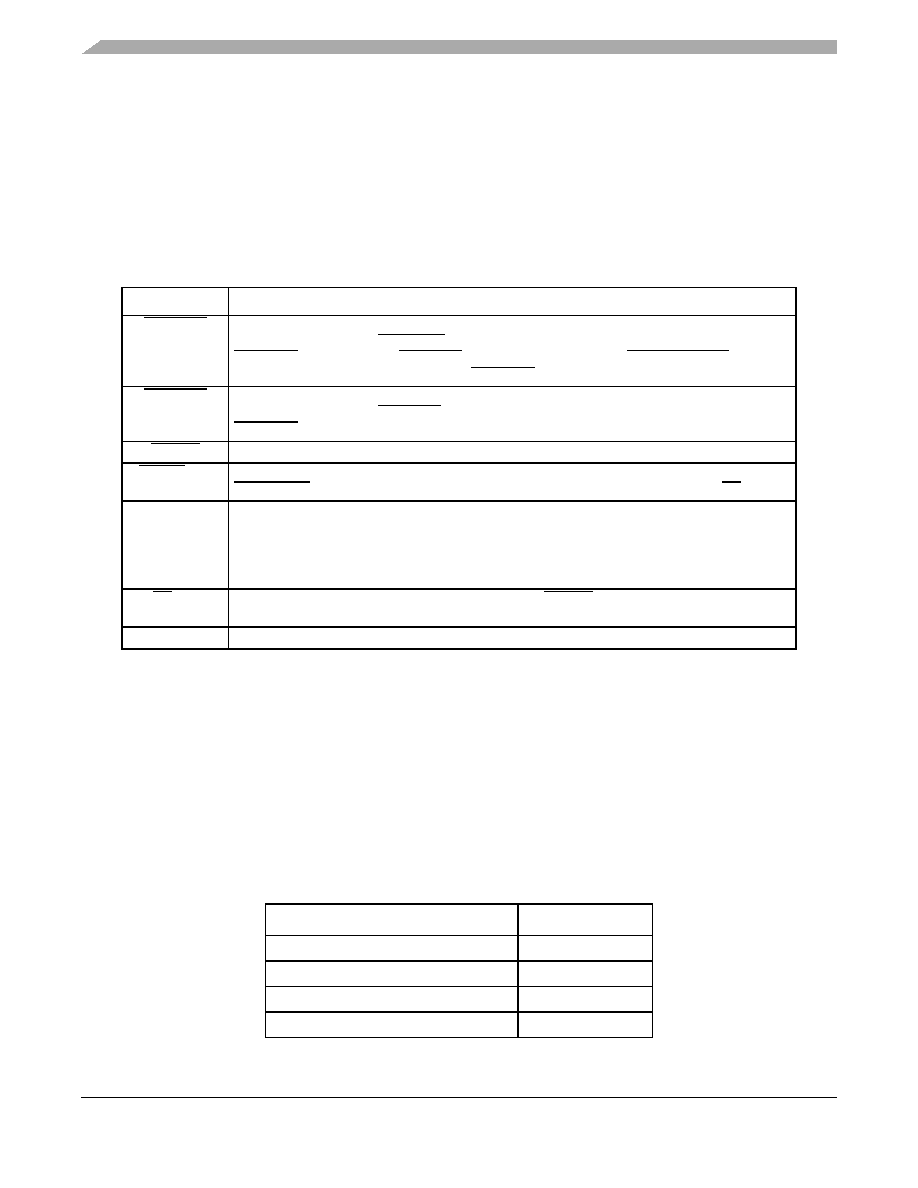
Table 3 shows the behavior of SDRAM signals in synchronous mode.
5.7.1.2
Address Multiplexing
See the SDRAM controller module chapter in the MCF5275 Reference Manual for details on address
multiplexing.
5.7.2
Ethernet PHY Transceiver Connection
The FEC supports an MII interface for 10/100 Mbps Ethernet and a seven-wire serial interface for 10 Mbps
Ethernet. The interface mode is selected by R_CNTRL[MII_MODE]. In MII mode, the 802.3 standard
defines and the FEC module supports 18 signals. These are shown in Table 4.
Table 3. Synchronous DRAM Signal Connections
Signal
Description
SD_SRAS
Synchronous row address strobe. Indicates a valid SDRAM row address is present and can be
latched by the SDRAM. SD_SRAS should be connected to the corresponding SDRAM
SD_SRAS. Do not confuse SD_SRAS with the DRAM controller’s SDRAM_CS[1:0], which
should not be interfaced to the SDRAM SD_SRAS signals.
SD_SCAS
Synchronous column address strobe. Indicates a valid column address is present and can be
latched by the SDRAM. SD_SCAS should be connected to the corresponding signal labeled
SD_SCAS on the SDRAM.
SD_WE
DRAM read/write. Asserted for write operations and negated for read operations.
SD_CS[1:0]
Row address strobe. Select each memory block of SDRAMs connected to the MCF5275. One
SDRAM_CS signal selects one SDRAM block and connects to the corresponding CS signals.
SD_CKE
Synchronous DRAM clock enable. Connected directly to the CKE (clock enable) signal of
SDRAMs. Enables and disables the clock internal to SDRAM. When CKE is low, memory can
enter a power-down mode where operations are suspended or they can enter self-refresh
mode. SD_CKE functionality is controlled by DCR[COC]. For designs using external
multiplexing, setting COC allows SD_CKE to provide command-bit functionality.
BS[3:2]
Column address strobe. For synchronous operation, BS[3:2] function as byte enables to the
SDRAMs. They connect to the DQM signals (or mask qualifiers) of the SDRAMs.
DDR_CLKOUT
Bus clock output. Connects to the CLK input of SDRAMs.
Table 4. MII Mode
Signal Description
MCF5275 Pin
Transmit clock
FECn_TXCLK
Transmit enable
FECn_TXEN
Transmit data
FECn_TXD[3:0]
Transmit error
FECn_TXER
相关PDF资料 |
PDF描述 |
|---|---|
| COP8SAC728N8/NOPB | IC MCU OTP 8BIT 4K 28DIP |
| MC9328MX21SCVMR2 | IC MPU I.MX21S 289-MAPBGA |
| VI-B73-IW-B1 | CONVERTER MOD DC/DC 24V 100W |
| MC9328MX21SCVM | IC MPU I.MX21S 289-MAPBGA |
| PK30X256VLQ100 | IC ARM CORTEX MCU 256K 144-LQFP |
相关代理商/技术参数 |
参数描述 |
|---|---|
| MCF5274LCVM166J | 制造商:Freescale Semiconductor 功能描述:MCF5275 V2CORE - Bulk |
| MCF5274LVF166 | 功能描述:微处理器 - MPU MCF5275 V2CORE RoHS:否 制造商:Atmel 处理器系列:SAMA5D31 核心:ARM Cortex A5 数据总线宽度:32 bit 最大时钟频率:536 MHz 程序存储器大小:32 KB 数据 RAM 大小:128 KB 接口类型:CAN, Ethernet, LIN, SPI,TWI, UART, USB 工作电源电压:1.8 V to 3.3 V 最大工作温度:+ 85 C 安装风格:SMD/SMT 封装 / 箱体:FBGA-324 |
| MCF5274LVM133 | 功能描述:IC MCU 32BIT 133MHZ 196-MAPBGA RoHS:否 类别:集成电路 (IC) >> 嵌入式 - 微控制器, 系列:MCF527x 标准包装:250 系列:56F8xxx 核心处理器:56800E 芯体尺寸:16-位 速度:60MHz 连通性:CAN,SCI,SPI 外围设备:POR,PWM,温度传感器,WDT 输入/输出数:21 程序存储器容量:40KB(20K x 16) 程序存储器类型:闪存 EEPROM 大小:- RAM 容量:6K x 16 电压 - 电源 (Vcc/Vdd):2.25 V ~ 3.6 V 数据转换器:A/D 6x12b 振荡器型:内部 工作温度:-40°C ~ 125°C 封装/外壳:48-LQFP 包装:托盘 配用:MC56F8323EVME-ND - BOARD EVALUATION MC56F8323 |
| MCF5274LVM166 | 功能描述:微处理器 - MPU MCF5274L V2CORE 64KSRAM RoHS:否 制造商:Atmel 处理器系列:SAMA5D31 核心:ARM Cortex A5 数据总线宽度:32 bit 最大时钟频率:536 MHz 程序存储器大小:32 KB 数据 RAM 大小:128 KB 接口类型:CAN, Ethernet, LIN, SPI,TWI, UART, USB 工作电源电压:1.8 V to 3.3 V 最大工作温度:+ 85 C 安装风格:SMD/SMT 封装 / 箱体:FBGA-324 |
| MCF5274LVM166 | 制造商:Freescale Semiconductor 功能描述:Microprocessor IC |
发布紧急采购,3分钟左右您将得到回复。