- 您现在的位置:买卖IC网 > PDF目录10952 > MCHC11F1CFNE2R (Freescale Semiconductor)MCU 8BIT 1KRAM 512EE 68-PLCC PDF资料下载
参数资料
| 型号: | MCHC11F1CFNE2R |
| 厂商: | Freescale Semiconductor |
| 文件页数: | 16/158页 |
| 文件大小: | 0K |
| 描述: | MCU 8BIT 1KRAM 512EE 68-PLCC |
| 标准包装: | 250 |
| 系列: | HC11 |
| 核心处理器: | HC11 |
| 芯体尺寸: | 8-位 |
| 速度: | 2MHz |
| 连通性: | SCI,SPI |
| 外围设备: | POR,WDT |
| 输入/输出数: | 30 |
| 程序存储器类型: | ROMless |
| EEPROM 大小: | 512 x 8 |
| RAM 容量: | 1K x 8 |
| 电压 - 电源 (Vcc/Vdd): | 4.75 V ~ 5.25 V |
| 数据转换器: | A/D 8x8b |
| 振荡器型: | 内部 |
| 工作温度: | -40°C ~ 85°C |
| 封装/外壳: | 68-LCC(J 形引线) |
| 包装: | 带卷 (TR) |
第1页第2页第3页第4页第5页第6页第7页第8页第9页第10页第11页第12页第13页第14页第15页当前第16页第17页第18页第19页第20页第21页第22页第23页第24页第25页第26页第27页第28页第29页第30页第31页第32页第33页第34页第35页第36页第37页第38页第39页第40页第41页第42页第43页第44页第45页第46页第47页第48页第49页第50页第51页第52页第53页第54页第55页第56页第57页第58页第59页第60页第61页第62页第63页第64页第65页第66页第67页第68页第69页第70页第71页第72页第73页第74页第75页第76页第77页第78页第79页第80页第81页第82页第83页第84页第85页第86页第87页第88页第89页第90页第91页第92页第93页第94页第95页第96页第97页第98页第99页第100页第101页第102页第103页第104页第105页第106页第107页第108页第109页第110页第111页第112页第113页第114页第115页第116页第117页第118页第119页第120页第121页第122页第123页第124页第125页第126页第127页第128页第129页第130页第131页第132页第133页第134页第135页第136页第137页第138页第139页第140页第141页第142页第143页第144页第145页第146页第147页第148页第149页第150页第151页第152页第153页第154页第155页第156页第157页第158页
TIMING SYSTEM
MC68HC11F1
9-6
TECHNICAL DATA
9.2.2 Timer Input Capture Registers
When an edge has been detected and synchronized, the 16-bit free-running counter
value is transferred into the input capture register pair as a single 16-bit parallel trans-
fer. Timer counter value captures and timer counter incrementing occur on opposite
half-cycles of the phase 2 clock so that the count value is stable whenever a capture
occurs. The TICx registers are not affected by reset. Input capture values can be read
from a pair of 8-bit read-only registers. A read of the high-order byte of an input capture
register pair inhibits a new capture transfer for one bus cycle. If a double-byte read in-
struction, such as LDD, is used to read the captured value, coherency is assured.
When a new input capture occurs immediately after a high-order byte read, transfer is
delayed for an additional cycle but the value is not lost.
TICx not affected by reset.
9.2.3 Timer Input Capture 4/Output Compare 5 Register
Use TI4/O5 as either an input capture register or an output compare register, depend-
ing on the function chosen for the PA3 pin. To enable it as an input capture pin, set the
I4/O5 bit in the pulse accumulator control register (PACTL) to logic level one. To use
it as an output compare register, set the I4/O5 bit to a logic level zero. Refer to 9.6
Pulse Accumulator.
The TI4/O5 register pair resets to ones ($FFFF).
9.3 Output Compare
Use the output compare (OC) function to program an action to occur at a specific time
— when the 16-bit counter reaches a specified value. For each of the five output com-
pare functions, there is a separate 16-bit compare register and a dedicated 16-bit com-
parator. The value in the compare register is compared to the value of the free-running
counter on every bus cycle. When the compare register matches the counter value, an
output compare status flag is set. The flag can be used to initiate the automatic actions
for that output compare function.
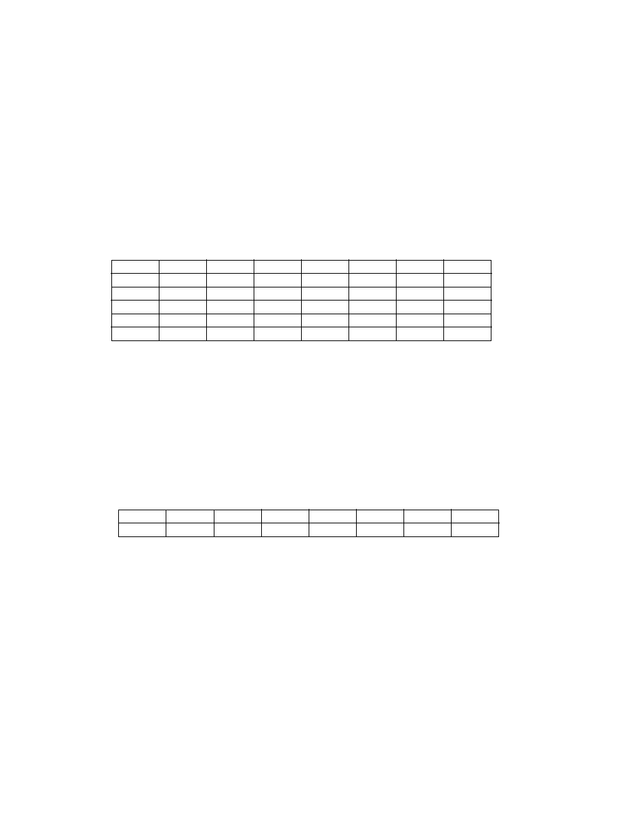
TIC1–TIC3 — Timer Input Capture
$1010–$1015
$1010
Bit 15
14
13
12
11
10
9
Bit 8
TIC1 (High)
$1011
Bit 7
654321
Bit 0
TIC1 (Low)
$1012
Bit 15
14
13
12
11
10
9
Bit 8
TIC2 (High)
$1013
Bit 7
654321
Bit 0
TIC2 (Low)
$1014
Bit 15
14
13
12
11
10
9
Bit 8
TIC3 (High)
$1015
Bit 7
654321
Bit 0
TIC3 (Low)
TI4/O5 — Timer Input Capture 4/Output Compare 5
$101E, $101F
$101E
Bit 15
14
13
12
11
10
9
Bit 8
TI4/O5 (High)
$101F
Bit 7
654321
Bit 0
TI4/O5 (Low)
F
re
e
sc
a
le
S
e
m
ic
o
n
d
u
c
to
r,
I
Freescale Semiconductor, Inc.
For More Information On This Product,
Go to: www.freescale.com
n
c
..
.
相关PDF资料 |
PDF描述 |
|---|---|
| MC9S12B128VPVE | IC MCU 128K FLASH 25MHZ 112-LQFP |
| MC908LJ24CFQE | IC MCU 24K FLASH 8MHZ SPI 80-QFP |
| B37981M5223K051 | CAP CER 0.022UF 50V 10% RADIAL |
| B37981F5223K051 | CAP CER 0.022UF 50V 10% RADIAL |
| VI-263-IY-F4 | CONVERTER MOD DC/DC 24V 50W |
相关代理商/技术参数 |
参数描述 |
|---|---|
| MCHC11F1CFNE3 | 功能描述:8位微控制器 -MCU 8B MCU 1KRAM 512EE RoHS:否 制造商:Silicon Labs 核心:8051 处理器系列:C8051F39x 数据总线宽度:8 bit 最大时钟频率:50 MHz 程序存储器大小:16 KB 数据 RAM 大小:1 KB 片上 ADC:Yes 工作电源电压:1.8 V to 3.6 V 工作温度范围:- 40 C to + 105 C 封装 / 箱体:QFN-20 安装风格:SMD/SMT |
| MCHC11F1CFNE3 | 制造商:Freescale Semiconductor 功能描述:8-Bit Microcontroller IC |
| MCHC11F1CFNE3R | 功能描述:8位微控制器 -MCU 8B MCU 1KRAM 512EE RoHS:否 制造商:Silicon Labs 核心:8051 处理器系列:C8051F39x 数据总线宽度:8 bit 最大时钟频率:50 MHz 程序存储器大小:16 KB 数据 RAM 大小:1 KB 片上 ADC:Yes 工作电源电压:1.8 V to 3.6 V 工作温度范围:- 40 C to + 105 C 封装 / 箱体:QFN-20 安装风格:SMD/SMT |
| MCHC11F1CFNE4 | 功能描述:8位微控制器 -MCU 8B MCU 1KRAM 512EE RoHS:否 制造商:Silicon Labs 核心:8051 处理器系列:C8051F39x 数据总线宽度:8 bit 最大时钟频率:50 MHz 程序存储器大小:16 KB 数据 RAM 大小:1 KB 片上 ADC:Yes 工作电源电压:1.8 V to 3.6 V 工作温度范围:- 40 C to + 105 C 封装 / 箱体:QFN-20 安装风格:SMD/SMT |
| MCHC11F1CFNE4R | 功能描述:8位微控制器 -MCU 8B MCU 1KRAM 512EE RoHS:否 制造商:Silicon Labs 核心:8051 处理器系列:C8051F39x 数据总线宽度:8 bit 最大时钟频率:50 MHz 程序存储器大小:16 KB 数据 RAM 大小:1 KB 片上 ADC:Yes 工作电源电压:1.8 V to 3.6 V 工作温度范围:- 40 C to + 105 C 封装 / 箱体:QFN-20 安装风格:SMD/SMT |
发布紧急采购,3分钟左右您将得到回复。