- 您现在的位置:买卖IC网 > PDF目录10950 > MCIMX351AVM4BR2 (Freescale Semiconductor)IC MPU I.MX35 400MAPBGA PDF资料下载
参数资料
| 型号: | MCIMX351AVM4BR2 |
| 厂商: | Freescale Semiconductor |
| 文件页数: | 107/147页 |
| 文件大小: | 0K |
| 描述: | IC MPU I.MX35 400MAPBGA |
| 标准包装: | 1,000 |
| 系列: | i.MX35 |
| 核心处理器: | ARM11 |
| 芯体尺寸: | 32-位 |
| 速度: | 400MHz |
| 连通性: | 1 线,CAN,EBI/EMI,以太网,I²C,MMC,SPI,SSI,UART/USART,USB OTG |
| 外围设备: | DMA,I²S,LCD,POR,PWM,WDT |
| 输入/输出数: | 96 |
| 程序存储器类型: | ROMless |
| RAM 容量: | 128K x 8 |
| 电压 - 电源 (Vcc/Vdd): | 1.22 V ~ 1.47 V |
| 振荡器型: | 外部 |
| 工作温度: | -40°C ~ 85°C |
| 封装/外壳: | 400-LFBGA |
| 包装: | 带卷 (TR) |
第1页第2页第3页第4页第5页第6页第7页第8页第9页第10页第11页第12页第13页第14页第15页第16页第17页第18页第19页第20页第21页第22页第23页第24页第25页第26页第27页第28页第29页第30页第31页第32页第33页第34页第35页第36页第37页第38页第39页第40页第41页第42页第43页第44页第45页第46页第47页第48页第49页第50页第51页第52页第53页第54页第55页第56页第57页第58页第59页第60页第61页第62页第63页第64页第65页第66页第67页第68页第69页第70页第71页第72页第73页第74页第75页第76页第77页第78页第79页第80页第81页第82页第83页第84页第85页第86页第87页第88页第89页第90页第91页第92页第93页第94页第95页第96页第97页第98页第99页第100页第101页第102页第103页第104页第105页第106页当前第107页第108页第109页第110页第111页第112页第113页第114页第115页第116页第117页第118页第119页第120页第121页第122页第123页第124页第125页第126页第127页第128页第129页第130页第131页第132页第133页第134页第135页第136页第137页第138页第139页第140页第141页第142页第143页第144页第145页第146页第147页
i.MX35 Applications Processors for Automotive Products, Rev. 10
Freescale Semiconductor
62
4.9.8
Fast Ethernet Controller (FEC) AC Electrical Specifications
This section describes the electrical information of the FEC module. The FEC is designed to support both
10- and 100-Mbps Ethernet networks. An external transceiver interface and transceiver function are
required to complete the interface to the media. The FEC supports the 10/100 Mbps Media Independent
Interface (MII) using a total of 18 pins. The 10-Mbps 7-wire interface that is restricted to a 10-Mbps data
rate uses seven of the MII pins for connection to an external Ethernet transceiver.
4.9.8.1
FEC AC Timing
This section describes the AC timing specifications of the FEC. The MII signals are compatible with
transceivers operating at a voltage of 3.3 V.
4.9.8.2
MII Receive Signal Timing
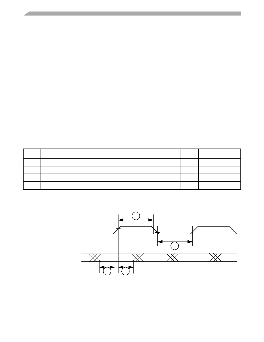
The MII receive timing signals consist of FEC_RXD[3:0], FEC_RX_DV, FEC_RX_ER, and
FEC_RX_CLK. The receiver functions correctly up to a FEC_RX_CLK maximum frequency of
25 MHz + 1%. There is no minimum frequency requirement. Additionally, the processor clock frequency
must exceed twice the FEC_RX_CLK frequency. Table 48 lists MII receive channel timings.
1 FEC_RX_DV, FEC_RX_CLK, and FEC_RXD0 have the same timing when in 10 Mbps 7-wire interface mode.
Figure 39. MII Receive Signal Timing Diagram
Table 48. MII Receive Signal Timing
Num.
Characteristic1
Min.
Max.
Unit
M1
FEC_RXD[3:0], FEC_RX_DV, FEC_RX_ER to FEC_RX_CLK setup
5
—
ns
M2
FEC_RX_CLK to FEC_RXD[3:0], FEC_RX_DV, FEC_RX_ER hold
5
—
ns
M3
FEC_RX_CLK pulse width high
35%
65%
FEC_RX_CLK period
M4
FEC_RX_CLK pulse width low
35%
65%
FEC_RX_CLK period
FEC_RX_CLK (input)
FEC_RXD[3:0] (inputs)
FEC_RX_DV
FEC_RX_ER
M3
M4
M1
M2
相关PDF资料 |
PDF描述 |
|---|---|
| VI-B6V-IW-B1 | CONVERTER MOD DC/DC 5.8V 100W |
| VI-2N3-IY-F3 | CONVERTER MOD DC/DC 24V 50W |
| MCIMX351AJQ5CR2 | MULTIMEDIA PROCESSOR 400-MAPBGA |
| VI-B5M-IX-B1 | CONVERTER MOD DC/DC 10V 75W |
| VI-2N2-IY-F2 | CONVERTER MOD DC/DC 15V 50W |
相关代理商/技术参数 |
参数描述 |
|---|---|
| MCIMX351AVM5B | 制造商:FREESCALE 制造商全称:Freescale Semiconductor, Inc 功能描述:Multimedia Applications Processor for Automotive Products |
| MCIMX353CJQ4C | 制造商:FREESCALE 制造商全称:Freescale Semiconductor, Inc 功能描述:i.MX35 Applications Processors for Industrial and Consumer Products |
| MCIMX353CJQ5C | 功能描述:处理器 - 专门应用 RINGO MX35 TO2.1 RoHS:否 制造商:Freescale Semiconductor 类型:Multimedia Applications 核心:ARM Cortex A9 处理器系列:i.MX6 数据总线宽度:32 bit 最大时钟频率:1 GHz 指令/数据缓存: 数据 RAM 大小:128 KB 数据 ROM 大小: 工作电源电压: 最大工作温度:+ 95 C 安装风格:SMD/SMT 封装 / 箱体:MAPBGA-432 |
| MCIMX353CJQ5CR2 | 功能描述:处理器 - 专门应用 RINGO MX35 TO2.1 RoHS:否 制造商:Freescale Semiconductor 类型:Multimedia Applications 核心:ARM Cortex A9 处理器系列:i.MX6 数据总线宽度:32 bit 最大时钟频率:1 GHz 指令/数据缓存: 数据 RAM 大小:128 KB 数据 ROM 大小: 工作电源电压: 最大工作温度:+ 95 C 安装风格:SMD/SMT 封装 / 箱体:MAPBGA-432 |
| MCIMX353CVM5B | 功能描述:处理器 - 专门应用 i.MX35 Auto Apps Processor RoHS:否 制造商:Freescale Semiconductor 类型:Multimedia Applications 核心:ARM Cortex A9 处理器系列:i.MX6 数据总线宽度:32 bit 最大时钟频率:1 GHz 指令/数据缓存: 数据 RAM 大小:128 KB 数据 ROM 大小: 工作电源电压: 最大工作温度:+ 95 C 安装风格:SMD/SMT 封装 / 箱体:MAPBGA-432 |
发布紧急采购,3分钟左右您将得到回复。