- 您现在的位置:买卖IC网 > Datasheet目录342 > MCP14E9T-E/MF (Microchip Technology)IC MOSFET DRIVER 3A 8DFN-S Datasheet资料下载
参数资料
| 型号: | MCP14E9T-E/MF |
| 厂商: | Microchip Technology |
| 文件页数: | 13/30页 |
| 文件大小: | 0K |
| 描述: | IC MOSFET DRIVER 3A 8DFN-S |
| 标准包装: | 3,300 |
| 配置: | 低端 |
| 输入类型: | 反相 |
| 延迟时间: | 45ns |
| 电流 - 峰: | 3A |
| 配置数: | 2 |
| 输出数: | 2 |
| 电源电压: | 4.5 V ~ 18 V |
| 工作温度: | -40°C ~ 125°C |
| 安装类型: | 表面贴装 |
| 封装/外壳: | 8-VDFN 裸露焊盘 |
| 供应商设备封装: | 8-DFN-S(6x5) |
| 包装: | 带卷 (TR) |
第1页第2页第3页第4页第5页第6页第7页第8页第9页第10页第11页第12页当前第13页第14页第15页第16页第17页第18页第19页第20页第21页第22页第23页第24页第25页第26页第27页第28页第29页第30页
�� �
�
�MCP14E9/10/11�
�4.0�
�APPLICATION� INFORMATION�
�4.1�
�General� Information�
�V� DD� =� 18V�
�MOSFET� drivers� are� high-speed,� high-current� devices�
�which� are� intended� to� source/sink� high-peak� currents� to�
�charge/discharge� the� gate� capacitance� of� external�
�MOSFETs,� or� insulated� gate� bipolar� transistors�
�(IGBTs).� In� high-frequency� switching� power� supplies,�
�the� Pulse-Width� Modulation� (PWM)� controller� may� not�
�have� the� drive� capability� to� directly� drive� the� power�
�MOSFET.� MOSFET� drivers,� like� the� MCP14E9/10/11�
�family,� can� be� used� to� provide� additional� source/sink�
�current� capability.�
�An� additional� degree� of� control� has� been� added� to� the�
�Input�
�Input�
�1� μF�
�MCP14E9�
�?� MCP14E11�
�0.1� μF�
�Ceramic�
�Output�
�C� L� =� 1800� pF�
�Output�
�C� L� =� 1800� pF�
�0V�
�t� D1� 90%�
�t� D2�
�MCP14E9/10/11� family.� There� are� seperate� enable�
�functions� for� each� driver� that� allow� for� the� immediate�
�termination� of� the� output� pulse,� regardless� of� the� state�
�of� the� input� signal.�
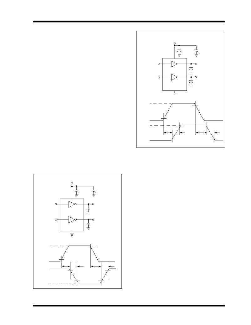
�4.2� MOSFET� Driver� Timing�
�The� ability� of� a� MOSFET� driver� to� transition� from� a� fully�
�OFF� state� to� a� fully� ON� state� are� characterized� by� the�
�drivers’� rise� time� (t� R� ),� fall� time� (t� F� )� and� propagation�
�delays� (t� D1� and� t� D2� ).� The� MCP14E9/10/11� family� of� driv-�
�ers� can� typically� charge� and� discharge� an� 1800� pF� load�
�capacitance� in� approximately� 15� ns,� along� with� a� typical�
�matched� propagation� delay� of� 45� ns.� Figure� 4-1� and�
�+5V�
�Input�
�10%�
�18V�
�Output�
�0V�
�FIGURE� 4-2:�
�Waveform.�
�90%�
�90%�
�t� R� t� F�
�10%� 10%�
�Non-Inverting� Driver� Timing�
�Figure� 4-2� show� the� test� circuit� and� timing� waveform�
�used� to� verify� the� MCP14E9/10/11� timing.�
�4.3�
�Enable� Function�
�The� ENB_A� and� ENB_B� enable� pins� allow� the� indepen-�
�Input�
�Input�
�V� DD� =� 18V�
�1� μF�
�MCP14E9�
�?� MCP14E11�
�0.1� μF�
�Ceramic�
�Output�
�C� L� =� 1800� pF�
�Output�
�C� L� =� 1800� pF�
�dent� control� of� OUT� A� and� OUT� B,� respectively.� They�
�are� active-high� and� are� internally� pulled� up� to� V� DD� ,� so�
�that� the� default� state� is� to� enable� the� driver.� These� pins�
�can� be� left� floating� for� normal� operation.�
�When� an� enable� pin� voltage� is� above� the� enable� pin�
�high� threshold� voltage,� V� EN_H� ,� that� driver� output� is�
�enabled� and� allowed� to� react� to� changes� in� the� INPUT�
�pin� voltage� state.� Similarly,� when� the� enable� pin� voltage�
�falls� below� the� enable� pin� low� threshold� voltage,� V� EN_L� ,�
�that� driver� output� is� disabled� and� does� not� respond� to�
�the� changes� in� the� INPUT� pin� voltage� state.� When� the�
�driver� is� disabled,� the� output� goes� to� a� low� state.� Refer�
�to� Table� 4-1� for� enable� pin� logic.� The� threshold� voltages�
�of� the� enable� function� are� compatible� with� logic� levels.�
�+5V�
�Input�
�0V� 10%�
�18V�
�Output�
�0V�
�t� D1�
�t� F�
�90%�
�10%�
�90%�
�t� D2�
�t� R�
�90%�
�10%�
�Hysteresis� is� provided� to� help� increase� the� noise� immu-�
�nity� of� the� enable� function,� avoiding� false� triggers� of� the�
�enable� signal� during� driver� switching.� For� robust�
�designs,� it� is� recommended� that� the� slew� rate� of� the�
�enable� pin� signal� be� greater� than� 1V/ns.�
�There� are� propagation� delays� associated� with� the�
�driver� receiving� an� enable� signal� and� the� output�
�reacting.� These� propagation� delays,� t� D3� and� t� D4� ,� are�
�graphically� represented� in� Figure� 4-3� .�
�FIGURE� 4-1:�
�Waveform.�
�Inverting� Driver� Timing�
�?� 2011� Microchip� Technology� Inc.�
�DS25005A-page� 13�
�相关PDF资料 |
PDF描述 |
|---|---|
| MCP1640RD-4ABC | BOARD REF DES AAAA BAT BOOST |
| MCP3906AT-E/SS | IC ENERGY METERING 24SSOP |
| MCP3907T-I/SS | IC ENERGY METER W/OSC 24SSOP |
| MCZ33198EF | IC TMOS DRIVER AUTO HISIDE 8SOIC |
| MCZ33285EFR2 | IC TMOS DRIVER DUAL HISIDE 8SOIC |
相关代理商/技术参数 |
参数描述 |
|---|---|
| MCP-14-I9-LL | 制造商:YAMAICHI 制造商全称:Yamaichi Electronics Co., Ltd. 功能描述:MatchCon |
| MCP-14-TI9-LL | 制造商:YAMAICHI 制造商全称:Yamaichi Electronics Co., Ltd. 功能描述:MatchCon |
| MCP1525 | 制造商:MICROCHIP 制造商全称:Microchip Technology 功能描述:2.5V and 4.096V Voltage References |
| MCP1525_05 | 制造商:MICROCHIP 制造商全称:Microchip Technology 功能描述:2.5V and 4.096V Voltage References |
| MCP1525_13 | 制造商:MICROCHIP 制造商全称:Microchip Technology 功能描述:2.5V and 4.096V Voltage References |
发布紧急采购,3分钟左右您将得到回复。