- 您现在的位置:买卖IC网 > PDF目录2159 > MCP6V11T-E/OT (Microchip Technology)IC OPAMP SGL ZERO DRIFT SOT23-5 PDF资料下载
参数资料
| 型号: | MCP6V11T-E/OT |
| 厂商: | Microchip Technology |
| 文件页数: | 15/40页 |
| 文件大小: | 0K |
| 描述: | IC OPAMP SGL ZERO DRIFT SOT23-5 |
| 标准包装: | 1 |
| 放大器类型: | 零漂移 |
| 电路数: | 1 |
| 输出类型: | 满摆幅 |
| 转换速率: | 0.03 V/µs |
| 增益带宽积: | 80kHz |
| 电流 - 输入偏压: | 5pA |
| 电压 - 输入偏移: | 8µV |
| 电流 - 电源: | 7.5µA |
| 电流 - 输出 / 通道: | 17mA |
| 电压 - 电源,单路/双路(±): | 1.6 V ~ 5.5 V |
| 工作温度: | -40°C ~ 125°C |
| 安装类型: | 表面贴装 |
| 封装/外壳: | SC-74A,SOT-753 |
| 供应商设备封装: | SOT-23-5 |
| 包装: | 标准包装 |
| 其它名称: | MCP6V11T-E/OTDKR |
第1页第2页第3页第4页第5页第6页第7页第8页第9页第10页第11页第12页第13页第14页当前第15页第16页第17页第18页第19页第20页第21页第22页第23页第24页第25页第26页第27页第28页第29页第30页第31页第32页第33页第34页第35页第36页第37页第38页第39页第40页
MCP6V11/1U
DS25124A-page 22
2012 Microchip Technology Inc.
4.3.4
SOURCE RESISTANCES
The input bias currents have two significant
components; switching glitches that dominate at room
temperature and below, and input ESD diode leakage
currents that dominate at +85°C and above.
Make the resistances seen by the inputs small and
equal. This minimizes the output offset caused by the
input bias currents.
The inputs should see a resistance on the order of 10
to 1 k at high frequencies (i.e., above 1 MHz). This
helps minimize the impact of switching glitches, which
are very fast, on overall performance. In some cases, it
may be necessary to add resistors in series with the
inputs to achieve this improvement in performance.
Small input resistances may be needed for high gains.
Without them, parasitic capacitances might cause
positive feedback and instability.
4.3.5
SOURCE CAPACITANCE
The capacitances seen by the two inputs should be
small and matched. The internal switches connected to
the inputs dump charges on these capacitors; an offset
can be created if the capacitances do not match. Large
input capacitances and source resistances, together
with high gain, can lead to positive feedback and
instability.
4.3.6
CAPACITIVE LOADS
Driving large capacitive loads can cause stability
problems for voltage feedback op amps. As the load
capacitance increases, the feedback loop’s phase
margin decreases and the closed-loop bandwidth is
reduced. This produces gain peaking in the frequency
response, with overshoot and ringing in the step
response. These zero-drift op amps have a different
output impedance than most op amps, due to their
unique topology.
When driving a capacitive load with these op amps, a
improves the feedback loop’s phase margin (stability)
by making the output load resistive at higher
frequencies. The bandwidth will be generally lower
than the bandwidth with no capacitive load.
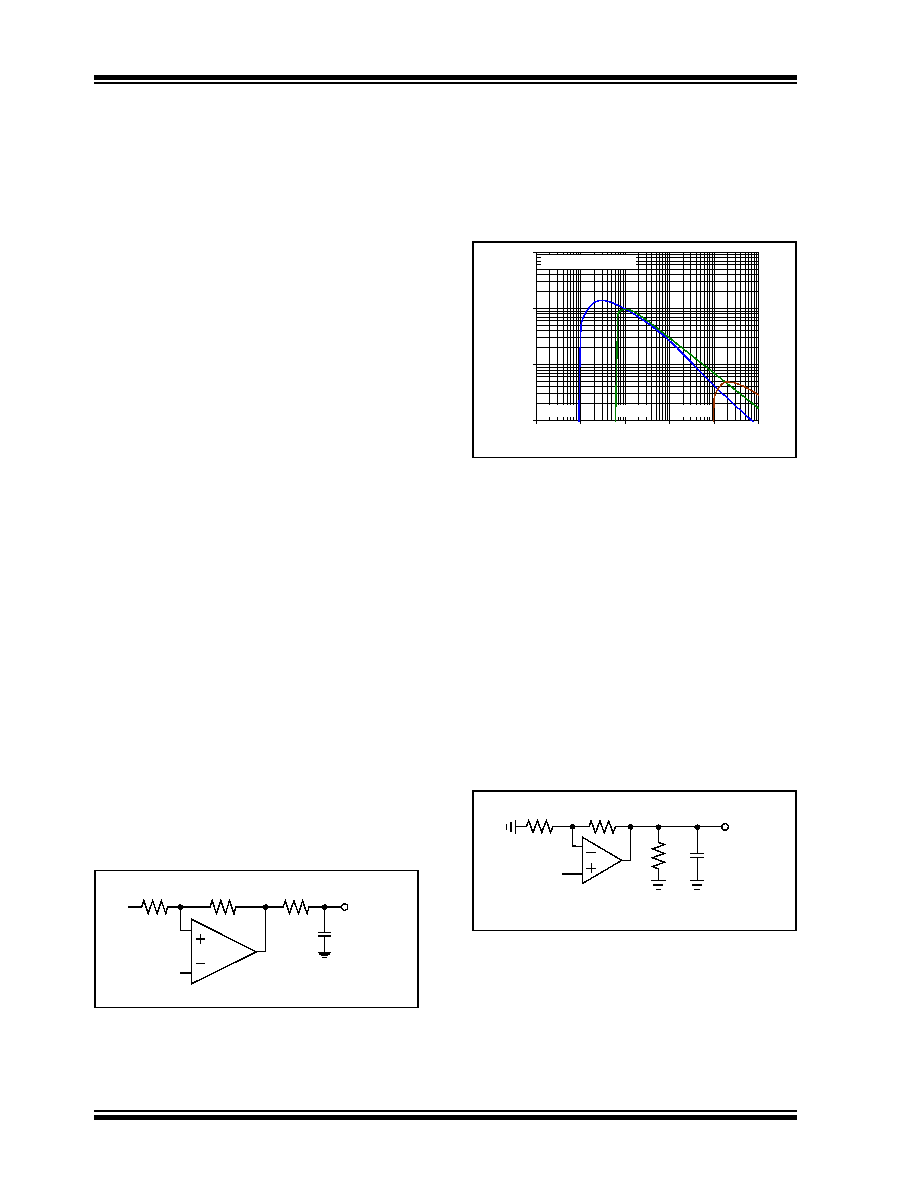
FIGURE 4-7:
Output Resistor, RISO,
Stabilizes Capacitive Loads.
different capacitive loads and gains. The x-axis is the
load capacitance (CL). The y-axis is the resistance
(RISO).
GN is the circuit’s noise gain. For non-inverting gains,
GN and the Signal Gain are equal. For inverting gains,
GN is 1+|Signal Gain| (e.g., -1 V/V gives GN = +2 V/V).
FIGURE 4-8:
Recommended RISO Values
for Capacitive Loads.
After selecting RISO for your circuit, double check the
resulting frequency response peaking and step
response overshoot. Modify RISO's value until the
response is reasonable. Bench evaluation is helpful.
4.3.7
STABILIZING OUTPUT LOADS
This family of zero-drift op amps has an output
impedance (Figure 2-31 and Figure 2-32) that has a
double zero when the gain is low. This can cause a
large phase shift in feedback networks that have low
impedance near the part’s bandwidth. This large phase
shift can cause stability problems.
Figure 4-9 shows that the load on the output is
(RL +RISO)||(RF +RG), where RISO is before the load
(like Figure 4-7). This load needs to be large enough to
maintain performance; it should be at least 10 k.
FIGURE 4-9:
Output Load.
RISO
CL
VOUT
U1
MCP6V1X
1E+03
1.E+04
1.E+05
m
mended
R
ISO
()
R
L||(RF + RG) 100 k
100k
10k
1k
1.E+02
1.E+03
1.E-11
1.E-10
1.E-09
1.E-08
1.E-07
1.E-06
Reco
m
Capacitive Load (F)
G
N = 1
G
N = 10
G
N = 100
100
1k
10p
100p
1n
10n
100n
1μ
RG
RF
VOUT
U1
MCP6V1X
RL
CL
相关PDF资料 |
PDF描述 |
|---|---|
| MCP6V27T-E/SN | IC OPAMP DUAL AUTO-ZERO 8SOIC |
| MCP6V31UT-E/LT | IC OPAMP SGL ZERO DRIFT SC70-5 |
| ME50101VX-000U-A99 | FAN BRUSHLESS 12VDC 50X50X10MM |
| MIC6211BM5 TR | IC OP AMP GEN PURPOSE SOT23-5 |
| MIC7111BM5 TR | IC OPAMP R-R I/O 1.8V SOT23-5 |
相关代理商/技术参数 |
参数描述 |
|---|---|
| MCP6V11UT-E/LT | 功能描述:运算放大器 - 运放 Single, Zero Drift Op Amp, E Temp RoHS:否 制造商:STMicroelectronics 通道数量:4 共模抑制比(最小值):63 dB 输入补偿电压:1 mV 输入偏流(最大值):10 pA 工作电源电压:2.7 V to 5.5 V 安装风格:SMD/SMT 封装 / 箱体:QFN-16 转换速度:0.89 V/us 关闭:No 输出电流:55 mA 最大工作温度:+ 125 C 封装:Reel |
| MCP6V11UT-E/LT-CUT TAPE | 制造商:Microchip Technology 功能描述:Cut Tape 制造商:Microchip Technology 功能描述:SP Amp Zero Drift Amplifier Single R-R I/O 5.5V 5-Pin SC-70 T/R |
| MCP6V11UT-E/OT | 功能描述:运算放大器 - 运放 Single, Zero Drift Op Amp, E Temp RoHS:否 制造商:STMicroelectronics 通道数量:4 共模抑制比(最小值):63 dB 输入补偿电压:1 mV 输入偏流(最大值):10 pA 工作电源电压:2.7 V to 5.5 V 安装风格:SMD/SMT 封装 / 箱体:QFN-16 转换速度:0.89 V/us 关闭:No 输出电流:55 mA 最大工作温度:+ 125 C 封装:Reel |
| MCP6V11UT-E/OT-CUT TAPE | 制造商:Microchip Technology 功能描述:Cut Tape 制造商:Microchip Technology 功能描述:SP Amp Zero Drift Amplifier Single R-R I/O 5.5V 5-Pin SOT-23 T/R |
| MCP6V26-E/MS | 功能描述:运算放大器 - 运放 Single, Auto-Zero Op Amp, E Temp RoHS:否 制造商:STMicroelectronics 通道数量:4 共模抑制比(最小值):63 dB 输入补偿电压:1 mV 输入偏流(最大值):10 pA 工作电源电压:2.7 V to 5.5 V 安装风格:SMD/SMT 封装 / 箱体:QFN-16 转换速度:0.89 V/us 关闭:No 输出电流:55 mA 最大工作温度:+ 125 C 封装:Reel |
发布紧急采购,3分钟左右您将得到回复。