- 您现在的位置:买卖IC网 > PDF目录2159 > MCP6V11T-E/OT (Microchip Technology)IC OPAMP SGL ZERO DRIFT SOT23-5 PDF资料下载
参数资料
| 型号: | MCP6V11T-E/OT |
| 厂商: | Microchip Technology |
| 文件页数: | 16/40页 |
| 文件大小: | 0K |
| 描述: | IC OPAMP SGL ZERO DRIFT SOT23-5 |
| 标准包装: | 1 |
| 放大器类型: | 零漂移 |
| 电路数: | 1 |
| 输出类型: | 满摆幅 |
| 转换速率: | 0.03 V/µs |
| 增益带宽积: | 80kHz |
| 电流 - 输入偏压: | 5pA |
| 电压 - 输入偏移: | 8µV |
| 电流 - 电源: | 7.5µA |
| 电流 - 输出 / 通道: | 17mA |
| 电压 - 电源,单路/双路(±): | 1.6 V ~ 5.5 V |
| 工作温度: | -40°C ~ 125°C |
| 安装类型: | 表面贴装 |
| 封装/外壳: | SC-74A,SOT-753 |
| 供应商设备封装: | SOT-23-5 |
| 包装: | 标准包装 |
| 其它名称: | MCP6V11T-E/OTDKR |
第1页第2页第3页第4页第5页第6页第7页第8页第9页第10页第11页第12页第13页第14页第15页当前第16页第17页第18页第19页第20页第21页第22页第23页第24页第25页第26页第27页第28页第29页第30页第31页第32页第33页第34页第35页第36页第37页第38页第39页第40页
2012 Microchip Technology Inc.
DS25124A-page 23
MCP6V11/1U
4.3.8
GAIN PEAKING
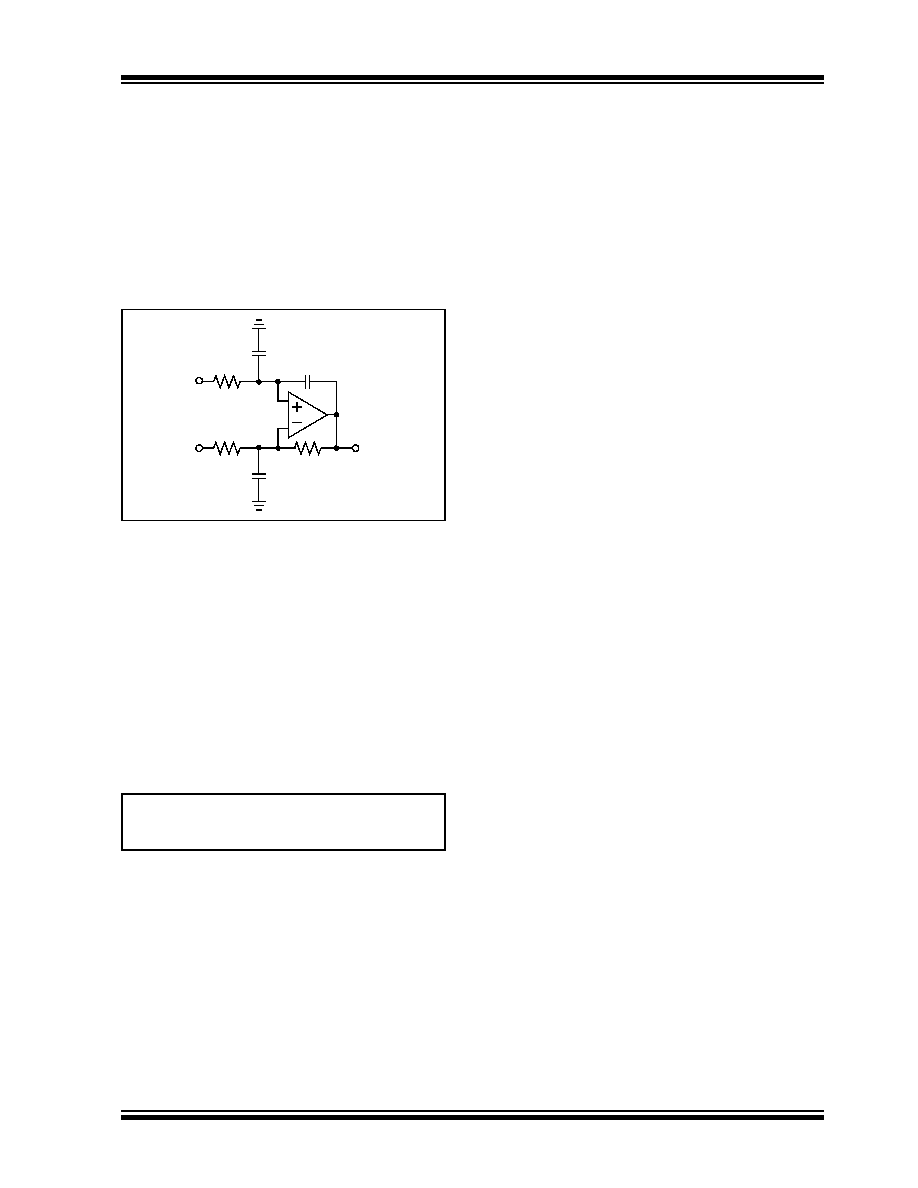
Figure 4-10 shows an op amp circuit that represents
non-inverting amplifiers (VM is a DC voltage and VP is
the input) or inverting amplifiers (VP is a DC voltage
and VM is the input). The capacitances CN and CG rep-
resent the total capacitance at the input pins; they
include the op amp’s common mode input capacitance
(CCM), board parasitic capacitance and any capacitor
placed in parallel. The capacitance CFP represents the
parasitic capacitance coupling the output and non-
inverting input pins.
FIGURE 4-10:
Amplifier with Parasitic
Capacitance.
CG acts in parallel with RG (except for a gain of +1 V/V),
which causes an increase in gain at high frequencies.
CG also reduces the phase margin of the feedback
loop, which becomes less stable. This effect can be
reduced by either reducing CG or RF||RG.
CN and RN form a low-pass filter that affects the signal
at VP. This filter has a single real pole at 1/(2πRNCN).
The largest value of RF that should be used depends
approximate limit for RF is:
EQUATION 4-2:
Some applications may modify these values to reduce
either output loading or gain peaking (step response
overshoot).
At high gains, RN needs to be small, in order to prevent
positive feedback and oscillations. Large CN values
can also help.
4.3.9
REDUCING UNDESIRED NOISE
AND SIGNALS
Reduce undesired noise and signals with:
Low bandwidth signal filters:
- Minimizes random analog noise
- Reduces interfering signals
Good PCB layout techniques:
- Minimizes crosstalk
- Minimizes parasitic capacitances and
inductances that interact with fast switching
edges
Good power supply design:
- Isolation from other parts
- Filtering of interference on supply line(s)
4.3.10
SUPPLY BYPASSING AND
FILTERING
With this family of operational amplifiers, the power
supply pin (VDD for single supply) should have a local
bypass capacitor (i.e., 0.01 F to 0.1 F) within 2 mm
of the pin for good high-frequency performance.
These parts also need a bulk capacitor (i.e., 1 F or
larger) within 100 mm to provide large, slow currents.
This bulk capacitor can be shared with other low noise,
analog parts.
In some cases, high-frequency power supply noise
(e.g., switched mode power supplies) may cause
undue intermodulation distortion, with a DC offset shift;
this noise needs to be filtered. Adding a resistor into the
supply connection can be helpful.
4.3.11
PCB DESIGN FOR DC PRECISION
In order to achieve DC precision on the order of ±1 V,
many physical errors need to be minimized. The design
of the Printed Circuit Board (PCB), the wiring, and the
thermal environment have a strong impact on the
precision achieved. A poor PCB design can easily be
more than 100 times worse than the MCP6V11/1U op
amps’ minimum and maximum specifications.
4.3.11.1
PCB Layout
Any time two dissimilar metals are joined together, a
temperature dependent voltage appears across the
junction (the Seebeck or thermojunction effect). This
effect is used in thermocouples to measure
temperature.
The
following
are
examples
of
thermojunctions on a PCB:
Components (resistors, op amps, …) soldered to
a copper pad
Wires mechanically attached to the PCB
Jumpers
Solder joints
PCB vias
RG
RF
VOUT
U1
MCP6V1X
CG
RN
CN
VM
VP
CFP
R
F
40 k
Ω
() 12 pF
C
G
--------------
×
G
N
2
×
≤
相关PDF资料 |
PDF描述 |
|---|---|
| MCP6V27T-E/SN | IC OPAMP DUAL AUTO-ZERO 8SOIC |
| MCP6V31UT-E/LT | IC OPAMP SGL ZERO DRIFT SC70-5 |
| ME50101VX-000U-A99 | FAN BRUSHLESS 12VDC 50X50X10MM |
| MIC6211BM5 TR | IC OP AMP GEN PURPOSE SOT23-5 |
| MIC7111BM5 TR | IC OPAMP R-R I/O 1.8V SOT23-5 |
相关代理商/技术参数 |
参数描述 |
|---|---|
| MCP6V11UT-E/LT | 功能描述:运算放大器 - 运放 Single, Zero Drift Op Amp, E Temp RoHS:否 制造商:STMicroelectronics 通道数量:4 共模抑制比(最小值):63 dB 输入补偿电压:1 mV 输入偏流(最大值):10 pA 工作电源电压:2.7 V to 5.5 V 安装风格:SMD/SMT 封装 / 箱体:QFN-16 转换速度:0.89 V/us 关闭:No 输出电流:55 mA 最大工作温度:+ 125 C 封装:Reel |
| MCP6V11UT-E/LT-CUT TAPE | 制造商:Microchip Technology 功能描述:Cut Tape 制造商:Microchip Technology 功能描述:SP Amp Zero Drift Amplifier Single R-R I/O 5.5V 5-Pin SC-70 T/R |
| MCP6V11UT-E/OT | 功能描述:运算放大器 - 运放 Single, Zero Drift Op Amp, E Temp RoHS:否 制造商:STMicroelectronics 通道数量:4 共模抑制比(最小值):63 dB 输入补偿电压:1 mV 输入偏流(最大值):10 pA 工作电源电压:2.7 V to 5.5 V 安装风格:SMD/SMT 封装 / 箱体:QFN-16 转换速度:0.89 V/us 关闭:No 输出电流:55 mA 最大工作温度:+ 125 C 封装:Reel |
| MCP6V11UT-E/OT-CUT TAPE | 制造商:Microchip Technology 功能描述:Cut Tape 制造商:Microchip Technology 功能描述:SP Amp Zero Drift Amplifier Single R-R I/O 5.5V 5-Pin SOT-23 T/R |
| MCP6V26-E/MS | 功能描述:运算放大器 - 运放 Single, Auto-Zero Op Amp, E Temp RoHS:否 制造商:STMicroelectronics 通道数量:4 共模抑制比(最小值):63 dB 输入补偿电压:1 mV 输入偏流(最大值):10 pA 工作电源电压:2.7 V to 5.5 V 安装风格:SMD/SMT 封装 / 箱体:QFN-16 转换速度:0.89 V/us 关闭:No 输出电流:55 mA 最大工作温度:+ 125 C 封装:Reel |
发布紧急采购,3分钟左右您将得到回复。