- 您现在的位置:买卖IC网 > PDF目录15517 > MIC2155YML TR (Micrel Inc)IC REG CTRLR BUCK PWM VM 32MLF PDF资料下载
参数资料
| 型号: | MIC2155YML TR |
| 厂商: | Micrel Inc |
| 文件页数: | 15/35页 |
| 文件大小: | 0K |
| 描述: | IC REG CTRLR BUCK PWM VM 32MLF |
| 特色产品: | MIC2155/6 Buck Control IC |
| 标准包装: | 1 |
| PWM 型: | 电压模式 |
| 输出数: | 1 |
| 频率 - 最大: | 550kHz |
| 占空比: | 80% |
| 电源电压: | 4.5 V ~ 14.5 V |
| 降压: | 是 |
| 升压: | 无 |
| 回扫: | 无 |
| 反相: | 无 |
| 倍增器: | 无 |
| 除法器: | 无 |
| Cuk: | 无 |
| 隔离: | 无 |
| 工作温度: | -40°C ~ 125°C |
| 封装/外壳: | 32-VFQFN 裸露焊盘,32-MLF? |
| 包装: | 标准包装 |
| 产品目录页面: | 1091 (CN2011-ZH PDF) |
| 其它名称: | 576-3527-6 |
第1页第2页第3页第4页第5页第6页第7页第8页第9页第10页第11页第12页第13页第14页当前第15页第16页第17页第18页第19页第20页第21页第22页第23页第24页第25页第26页第27页第28页第29页第30页第31页第32页第33页第34页第35页
�� �
�
�Micrel,� Inc.�
�Oscillator� and� Frequency� Synchronization�
�The� internal� oscillator� free� runs� at� a� fixed� frequency� and�
�requires� no� external� components.� The� oscillator�
�generates� two� clock� signals� that� are� 180°� out� of� phase�
�with� each� other.� This� forces� each� channel� of� the�
�controller� to� switch� 180°� out� of� phase,� which� reduces�
�input� and� output� ripple� current.�
�The� internal� oscillator� generates� a� clock� signal� and� ramp�
�signal.� The� clock� signal� terminates� the� switching� cycle�
�MIC2155/2156�
�with� an� appropriate� V� GS� threshold� should� be� used� in� this�
�situation.�
�The� voltage� on� the� bootstrap� capacitor� drops� each� time�
�it� delivers� charge� to� turn� on� the� MOSFET.� The� voltage�
�drop� depends� on� the� gate� charge� required� by� the�
�MOSFET.� Most� MOSFET� specifications� specify� gate�
�charge� vs.� V� GS� voltage.� Based� on� this� information� and� a�
�recommended� Δ� VHB� of� less� than� 0.1V,� the� minimum�
�value� of� bootstrap� capacitance� is� calculated� as:�
�for� each� channel.� The� ramp� voltage� for� Channel� 1� is�
�compared� with� the� output� of� the� error� amplifier� and�
�regulates� the� output� voltage.� The� ramp� signal� for�
�Channel� 2� is� compared� with� the� Channel� 2� error�
�C� BST� ≥�
�Q� GATE�
�Δ� V� BST�
�amplifier� output� and� forces� the� output� current� of� Channel�
�2� to� match� Channel� 1.�
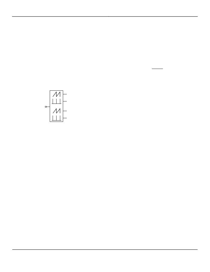
�RMP1�
�CLK1�
�SYNC�
�RMP2�
�CLK2�
�2� Phase�
�Oscillator�
�Figure� 8.� Oscillator� and� Sync� Diagram�
�The� SYNC� input� (pin� 15)� allows� the� MIC2155/6� to�
�synchronize� to� an� external� clock� signal.� When�
�synchronized,� each� channel� switches� at� half� of� the�
�synchronization� frequency.� Limitations� on� the�
�synchronization� frequency� and� signal� amplitude� are�
�listed� in� the� electrical� characteristics� section� of� the� spec.�
�When� not� used,� the� sync� pin� should� be� left� open� (no�
�connect).�
�MOSFET� Gate-Drive� Circuitry�
�The� high-side� drive� circuit� is� designed� to� switch� an� N-�
�channel� MOSFET.� Figure� 9� shows� a� diagram� of� the� gate�
�drive� and� bootstrap� circuit.� D2� and� C� BST� comprise� the�
�bootstrap� circuit,� which� is� used� to� supply� drive� voltage� to�
�the� high-side� FET.� Bootstrap� capacitor� C� BST� is� charged�
�through� diode� D2� while� the� low-side� MOSFET� is� on� and�
�the� voltage� on� the� SW� pin� is� approximately� 0V.� When�
�the� high-side� MOSFET� driver� is� turned� on,� energy� from�
�C� BST� is� used� to� charge� the� MOSFET� gate,� turning� on� the�
�FET.� As� the� MOSFET� turns� on,� the� voltage� on� the� SW�
�pin� increases� to� approximately� V� IN� .� Diode� D2� is� reversed�
�biased� and� C� BST� is� pulled� high� while� continuing� to� keep�
�the� high-side� MOSFET� on.� The� high-side� drive� voltage,�
�which� is� derived� from� V� DD� ,� is� approximately� 4.5V� due� the�
�voltage� drop� across� D2.� When� operating� at� 4.5V� IN� ,�
�without� connecting� V� DD� to� V� IN� ,� the� gate� drive� voltage� to�
�the� high-side� FET� could� be� as� low� as� 3.2V.� MOSFETs�
�Where:�
�Q� GATE� =� Total� Gate� Charge� a� V� BST�
�Δ� V� BST� =� Voltage� drop� at� the� BST� pin�
�A� minimum� value� of� 0.1μF� is� required� for� each� of� the�
�bootstrap� capacitors,� regardless� of� the� MOSFETs� being�
�driven.� Larger� or� paralleled� MOSFETs� may� require�
�larger� capacitance� values� for� proper� operation.�
�Placement� is� critical.� The� bypass� capacitor� (C� BST� )� for� the�
�BST� supply� pins� must� be� located� close� between� the� BST�
�and� SW1� pins.� The� etch� connections� should� be� short,�
�wide� and� direct.� The� use� of� a� ground� plane� to� minimize�
�connection� impedance� is� recommended.� Refer� to� the�
�section� on� layout� and� component� placement� for� more�
�information.�
�A� delay� between� the� switching� of� the� two� MOSFETs� is�
�necessary� to� prevent� both� MOSFETs� from� being� on� at�
�the� same� time� and� shorting� V� IN� to� ground.� An� adaptive�
�gate� drive� in� the� controller� monitors� the� switch� node�
�(SW1)� and� low-side� driver� (LSD1)� to� minimize� dead� time�
�while� preventing� both� MOSFETs� from� being� on� at� the�
�same� time.� This� enables� the� use� of� a� broad� range� of�
�MOSFETS� without� requiring� excessive� deadtime.�
�November� 2009�
�15�
�M9999-111209-B�
�相关PDF资料 |
PDF描述 |
|---|---|
| 4590-394K | INDUCTOR HIGH CURRENT 390.0UH |
| 4590-334K | INDUCTOR HIGH CURRENT 330.0UH |
| 4590-274K | INDUCTOR HIGH CURRENT 270.0UH |
| 4590R-184K | INDUCTOR HIGH CURRENT 180.0UH |
| 4590-184K | INDUCTOR HIGH CURRENT 180.0UH |
相关代理商/技术参数 |
参数描述 |
|---|---|
| MIC2156 | 制造商:MICREL 制造商全称:Micrel Semiconductor 功能描述:Two-Phase, Single-Output, PWM Synchronous Buck Control IC |
| MIC2156YML | 制造商:MICREL 制造商全称:Micrel Semiconductor 功能描述:2-Phase, Single Output, PWM Synchronous Buck Control IC |
| MIC2156YML TR | 功能描述:DC/DC 开关控制器 Single Output, PWM Sync Buck Controller RoHS:否 制造商:Texas Instruments 输入电压:6 V to 100 V 开关频率: 输出电压:1.215 V to 80 V 输出电流:3.5 A 输出端数量:1 最大工作温度:+ 125 C 安装风格: 封装 / 箱体:CPAK |
| MIC2156YML-TR | 功能描述:Buck Regulator Positive Output Step-Down DC-DC Controller IC 32-MLF? (5x5) 制造商:microchip technology 系列:- 包装:剪切带(CT) 零件状态:过期 输出类型:晶体管驱动器 功能:降压 输出配置:正 拓扑:降压 输出数:2 输出阶段:2 电压 - 电源(Vcc/Vdd):4.5 V ~ 14.5 V 频率 - 开关:300kHz 占空比(最大):0.8 同步整流器:是 时钟同步:是 串行接口:- 控制特性:限流,使能,电源良好,软启动 工作温度:-40°C ~ 125°C (TJ) 封装/外壳:32-VFQFN 裸露焊盘,32-MLF? 供应商器件封装:32-MLF?(5x5) 标准包装:1 |
| MIC2159 | 制造商:MICREL 制造商全称:Micrel Semiconductor 功能描述:SYNCHRONOUS-itty⑩ Step-Down Converter IC |
发布紧急采购,3分钟左右您将得到回复。