- 您现在的位置:买卖IC网 > PDF目录15517 > MIC2155YML TR (Micrel Inc)IC REG CTRLR BUCK PWM VM 32MLF PDF资料下载
参数资料
| 型号: | MIC2155YML TR |
| 厂商: | Micrel Inc |
| 文件页数: | 27/35页 |
| 文件大小: | 0K |
| 描述: | IC REG CTRLR BUCK PWM VM 32MLF |
| 特色产品: | MIC2155/6 Buck Control IC |
| 标准包装: | 1 |
| PWM 型: | 电压模式 |
| 输出数: | 1 |
| 频率 - 最大: | 550kHz |
| 占空比: | 80% |
| 电源电压: | 4.5 V ~ 14.5 V |
| 降压: | 是 |
| 升压: | 无 |
| 回扫: | 无 |
| 反相: | 无 |
| 倍增器: | 无 |
| 除法器: | 无 |
| Cuk: | 无 |
| 隔离: | 无 |
| 工作温度: | -40°C ~ 125°C |
| 封装/外壳: | 32-VFQFN 裸露焊盘,32-MLF? |
| 包装: | 标准包装 |
| 产品目录页面: | 1091 (CN2011-ZH PDF) |
| 其它名称: | 576-3527-6 |
第1页第2页第3页第4页第5页第6页第7页第8页第9页第10页第11页第12页第13页第14页第15页第16页第17页第18页第19页第20页第21页第22页第23页第24页第25页第26页当前第27页第28页第29页第30页第31页第32页第33页第34页第35页
�� �
�
�f� '� =� 1�
�Micrel,� Inc.�
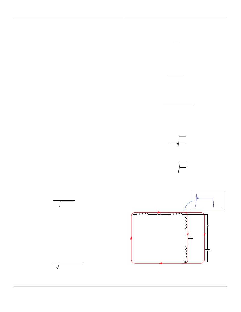
�One� method� of� reducing� the� ringing� is� to� use� a� resistor�
�and� capacitor� to� lower� the� Q� of� the� resonant� circuit.� The�
�circuit� in� Figure� 23� shows� the� resistor� in� between� the�
�switch� node� and� ground.� Capacitor� Cs� is� used� to� block�
�DC� and� minimize� the� power� dissipation� in� the� resistor.�
�This� capacitor� value� should� be� between� 5� and� 10� times�
�the� parasitic� capacitance� of� the� MOSFET� C� OSS� .� A�
�capacitor� that� is� too� small� will� have� high� impedance� and�
�prevent� the� resistor� from� damping� the� ringing.� A�
�capacitor� that� is� too� large� causes� unnecessary� power�
�MIC2155/2156�
�Define� f’� as:�
�f�
�f� 2�
�Combining� the� equations� for� f� 1� ,� f� 2� and� f’� to� derive� C� P� ,� the�
�parasitic� capacitance:�
�2� � (� f� )� 2� ?� 1�
�dissipation� in� the� resistor,� which� lowers� efficiency.�
�The� snubber� components� should� be� placed� as� close� as�
�possible� to� the� low-side� MOSFET� and/or� external�
�C� P� =�
�C� S�
�'�
�schottky� diode� since� in� contributes� to� most� of� the� stray�
�capacitance.� Placing� the� snubber� too� far� from� the� FET� or�
�using� etch� that� is� too� long� or� thin� will� add� inductance� to�
�L� P� is� solved� by� re-arranging� the� equation� for� f� 1� :�
�(� 2� π� )�
�the� snubber� and� diminishes� its� effectiveness.�
�A� proper� snubber� design� requires� the� parasitic�
�inductance� and� capacitance� be� known.� A� method� of�
�L� P� =�
�2�
�1�
�� C� P� � (� f� 1� )� 2�
�determining� these� values� and� calculating� the� damping�
�resistor� value� is� outlined� below.�
�Step� 3:� Calculate� the� damping� resistor.�
�Q� =�
�1.� Measure� the� ringing� frequency� at� the� switch� node�
�which� is� determined� by� parasitic� L� P� and� C� P� .� Define� this�
�frequency� as� f� 1� .�
�2.� Add� a� capacitor� C� S� (normally� at� least� 3� times� as� big� as�
�the� C� OSS� of� the� FET)� from� the� switch� node� to� ground� and�
�measure� the� new� ringing� frequency.� Define� this� new�
�(lower)� frequency� as� f� 2� .� L� P� and� C� P� can� now� be� solved�
�using� the� values� of� f� 1� ,� f� 2� and� C� S� .�
�Critical� damping� occurs� at� Q� =� 1:�
�1� L� P�
�R� S� C� S�
�Solving� for� R� S�
�=� 1�
�3.� Add� a� resistor� R� S� in� series� with� C� S� to� generate� critical�
�damping.�
�Step� 1:� First� measure� the� ringing� frequency� on� the�
�R� S� =�
�L� P�
�C� S�
�switch� node� voltage� when� the� high-side� MOSFET� turns�
�on.� This� ringing� is� characterized� by� the� equation:�
�Figure� 23� shows� the� snubber� in� the� circuit� and� the�
�damped� switch� node� waveform.�
�f� 1� =�
�1�
�2� π� L� P� ×� C� P�
�L� STRAY1�
�L� STRAY2�
�Where:�
�C� P� and� L� P� are� the� parasitic� capacitance� and�
�inductance�
�Step� 2:� Add� a� capacitor,� C� S� ,� in� parallel� with� the�
�synchronous� MOSFET,� Q2.� The� capacitor� value� should�
�be� approximately� 3� times� the� C� OSS� of� Q2.� Measure� the�
�frequency� of� the� switch� node� ringing,� f� 2� :�
�R� DS�
�L� STRAY3�
�C� OSS2�
�L� STRAY4�
�R� S�
�C� S�
�f� 2� =�
�November� 2009�
�1�
�2� π� Lp� ×� (� Cs� +� Cp� )�
�27�
�Figure� 23.� Snubber� Circuit�
�M9999-111209-B�
�相关PDF资料 |
PDF描述 |
|---|---|
| 4590-394K | INDUCTOR HIGH CURRENT 390.0UH |
| 4590-334K | INDUCTOR HIGH CURRENT 330.0UH |
| 4590-274K | INDUCTOR HIGH CURRENT 270.0UH |
| 4590R-184K | INDUCTOR HIGH CURRENT 180.0UH |
| 4590-184K | INDUCTOR HIGH CURRENT 180.0UH |
相关代理商/技术参数 |
参数描述 |
|---|---|
| MIC2156 | 制造商:MICREL 制造商全称:Micrel Semiconductor 功能描述:Two-Phase, Single-Output, PWM Synchronous Buck Control IC |
| MIC2156YML | 制造商:MICREL 制造商全称:Micrel Semiconductor 功能描述:2-Phase, Single Output, PWM Synchronous Buck Control IC |
| MIC2156YML TR | 功能描述:DC/DC 开关控制器 Single Output, PWM Sync Buck Controller RoHS:否 制造商:Texas Instruments 输入电压:6 V to 100 V 开关频率: 输出电压:1.215 V to 80 V 输出电流:3.5 A 输出端数量:1 最大工作温度:+ 125 C 安装风格: 封装 / 箱体:CPAK |
| MIC2156YML-TR | 功能描述:Buck Regulator Positive Output Step-Down DC-DC Controller IC 32-MLF? (5x5) 制造商:microchip technology 系列:- 包装:剪切带(CT) 零件状态:过期 输出类型:晶体管驱动器 功能:降压 输出配置:正 拓扑:降压 输出数:2 输出阶段:2 电压 - 电源(Vcc/Vdd):4.5 V ~ 14.5 V 频率 - 开关:300kHz 占空比(最大):0.8 同步整流器:是 时钟同步:是 串行接口:- 控制特性:限流,使能,电源良好,软启动 工作温度:-40°C ~ 125°C (TJ) 封装/外壳:32-VFQFN 裸露焊盘,32-MLF? 供应商器件封装:32-MLF?(5x5) 标准包装:1 |
| MIC2159 | 制造商:MICREL 制造商全称:Micrel Semiconductor 功能描述:SYNCHRONOUS-itty⑩ Step-Down Converter IC |
发布紧急采购,3分钟左右您将得到回复。