- 您现在的位置:买卖IC网 > PDF目录45328 > MK2049-11SI 56 MHz, OTHER CLOCK GENERATOR, PDSO20 PDF资料下载
参数资料
| 型号: | MK2049-11SI |
| 元件分类: | 时钟产生/分配 |
| 英文描述: | 56 MHz, OTHER CLOCK GENERATOR, PDSO20 |
| 封装: | 0.300 INCH, SOIC-20 |
| 文件页数: | 9/13页 |
| 文件大小: | 166K |
| 代理商: | MK2049-11SI |
Communications Clock PLL
MDS 2049-11 C
5
Revision 021402
Integrated Circuit Systems, Inc. q 525 Race Street San Jose, CA 95126 q tel (408) 295-9800 q
www.icst.com
MK2049-11
(see also notes below regarding C2) which may be
required for network clock wander transfer compliance.
A high damping factor may also increase output clock
jitter when there is excess digital noise in the system
application, due to the reduced ability of the PLL to
respond to and therefore compensate for phase noise
ingress.
Notes on setting the value of C2
As another general rule, the following relationship
should be maintained between components C1 and C2
in the loop filter:
C2 establishes a second pole in the VCXO PLL loop
filter. For higher damping factors (> 1), calculate the
value of C2 based on a C1 value that would be used for
a damping factor of 1. This will prevent excessive
baseband peaking and loop instability that can lead to
output jitter.
C2 also dampens VCXO input voltage modulation by
the charge pump correction pulses. A C2 value that is
too low will result in increased output phase noise at
the phase detector frequency due to this. In extreme
cases where input jitter is high, charge pump current is
high, and C2 is too small, the VCXO input voltage can
hit the supply or ground rail resulting in non-linear loop
response.
The best way to set the value of C2 is to use the filter
response software available from ICS (please refer to
the following section). C2 should be increased in value
until it just starts affecting the passband peak.
Loop Filter Response Software
ICS has a PC-based program available that simulates
VCXO PLL loop response characteristics. This can be
used instead of the above bandwidth and damping
factor equations. The user enters external loop filter
component values and other listed device
characteristics. The program generates a PLL
frequency response graph, which translates to jitter
attenuation characteristics. Normalized bandwidth
(NBW) and damping factor values are also calculated.
To obtain this free software please contact the
applications department of ICS, MicroClock Division, at
(408) 297-1201.
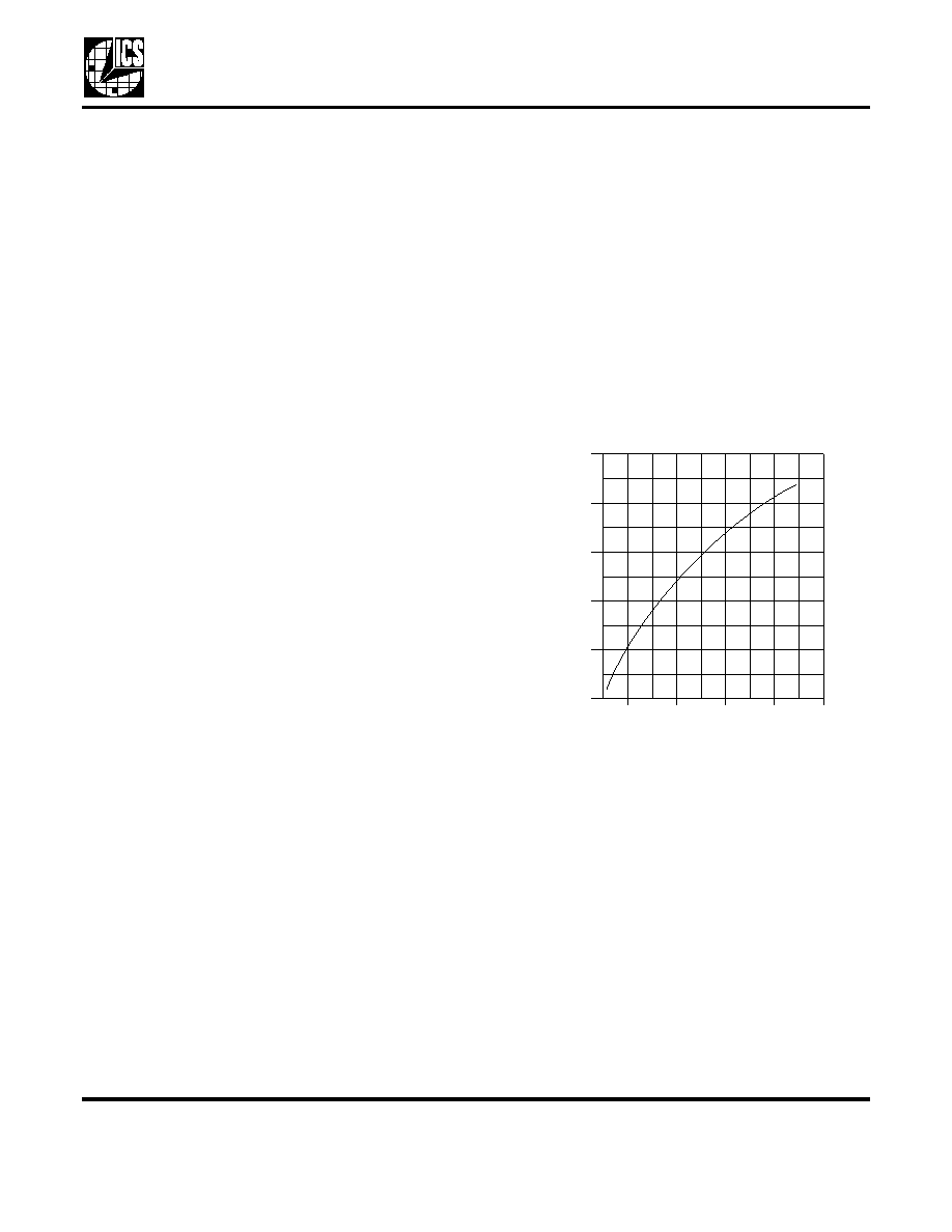
VCXO Gain (KO) vs. XTAL Frequency
C
2
C
1
20
------
=
10
20
15
25
30
2000
3000
4000
5000
6000
1000
C rystal Frequ en cy, M H z
V
C
X
O
G
a
in
(
K
O
),
H
z
p
e
r
V
o
lt
相关PDF资料 |
PDF描述 |
|---|---|
| MK2049-45ASI | 125 MHz, OTHER CLOCK GENERATOR, PDSO20 |
| MK2069-01GILFTR | 160 MHz, OTHER CLOCK GENERATOR, PDSO56 |
| MK2069-01GITR | 160 MHz, OTHER CLOCK GENERATOR, PDSO56 |
| MK2069-01GI | 160 MHz, OTHER CLOCK GENERATOR, PDSO56 |
| MK2069-02GILF | 160 MHz, OTHER CLOCK GENERATOR, PDSO56 |
相关代理商/技术参数 |
参数描述 |
|---|---|
| MK2049-34 | 制造商:ICS 制造商全称:ICS 功能描述:3.3 V Communications Clock PLL |
| MK2049-34A | 制造商:ICS 制造商全称:ICS 功能描述:3.3 Volt Communications Clock VCXO PLL |
| MK2049-34SAI | 功能描述:IC VCXO PLL CLK SYNTH 20-SOIC RoHS:否 类别:集成电路 (IC) >> 时钟/计时 - 时钟发生器,PLL,频率合成器 系列:- 标准包装:39 系列:- 类型:* PLL:带旁路 输入:时钟 输出:时钟 电路数:1 比率 - 输入:输出:1:10 差分 - 输入:输出:是/是 频率 - 最大:170MHz 除法器/乘法器:无/无 电源电压:2.375 V ~ 3.465 V 工作温度:0°C ~ 70°C 安装类型:* 封装/外壳:* 供应商设备封装:* 包装:* |
| MK2049-34SAILF | 功能描述:时钟合成器/抖动清除器 3.3 VOLT COMMUNICA. CLOCK VCXO PLL RoHS:否 制造商:Skyworks Solutions, Inc. 输出端数量: 输出电平: 最大输出频率: 输入电平: 最大输入频率:6.1 GHz 电源电压-最大:3.3 V 电源电压-最小:2.7 V 封装 / 箱体:TSSOP-28 封装:Reel |
| MK2049-34SAILFTR | 功能描述:时钟合成器/抖动清除器 3.3 VOLT COMMUNICA. CLOCK VCXO PLL RoHS:否 制造商:Skyworks Solutions, Inc. 输出端数量: 输出电平: 最大输出频率: 输入电平: 最大输入频率:6.1 GHz 电源电压-最大:3.3 V 电源电压-最小:2.7 V 封装 / 箱体:TSSOP-28 封装:Reel |
发布紧急采购,3分钟左右您将得到回复。