- 您现在的位置:买卖IC网 > PDF目录95978 > MMDF3N06VLR2 (MOTOROLA INC) 3.3 A, 60 V, 0.13 ohm, 2 CHANNEL, N-CHANNEL, Si, POWER, MOSFET PDF资料下载
参数资料
| 型号: | MMDF3N06VLR2 |
| 厂商: | MOTOROLA INC |
| 元件分类: | JFETs |
| 英文描述: | 3.3 A, 60 V, 0.13 ohm, 2 CHANNEL, N-CHANNEL, Si, POWER, MOSFET |
| 封装: | CASE 751-06, SO-8 |
| 文件页数: | 1/4页 |
| 文件大小: | 80K |
| 代理商: | MMDF3N06VLR2 |
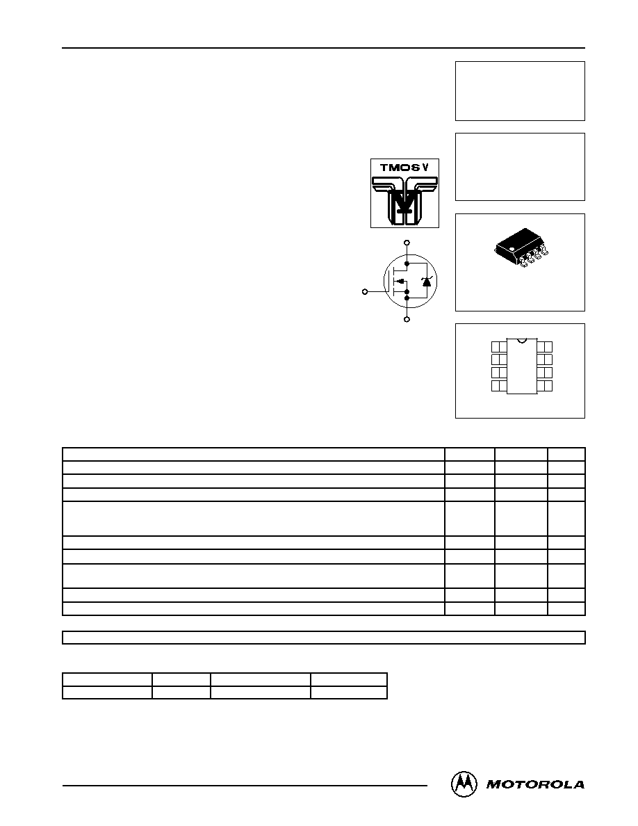
MMDF3N06VL
DUAL TMOS MOSFET
3.3 AMPERES
60 VOLTS
RDS(on) = 0.130 OHM
Source–1
1
2
3
4
8
7
6
5
Top View
Gate–1
Source–2
Gate–2
Drain–1
Drain–2
D
S
G
CASE 751–06, Style 11
SO–8
TM
1
Motorola TMOS Power MOSFET Transistor Device Data
Product Preview
TMOS V
SO-8 for Surface Mount
N–Channel Enhancement–Mode Silicon Gate
TMOS V is a new technology designed to achieve an on–resis-
tance area product about one–half that of standard MOSFETs. This
new technology more than doubles the present cell density of our
50 and 60 volt TMOS devices. Just as with our TMOS E–FET
designs, TMOS V is designed to withstand high energy in the
avalanche and commutation modes. Designed for low voltage, high
speed switching applications in power supplies, converters and
power motor controls, these devices are particularly well suited for
bridge circuits where diode speed and commutating safe operating
areas are critical and offer additional safety margin against
unexpected voltage transients.
New Features of TMOS V
On–resistance Area Product about One–half that of Standard
MOSFETs with New Low Voltage, Low RDS(on) Technology
Faster Switching than E–FET Predecessors
Features Common to TMOS V and TMOS E–FETS
Avalanche Energy Specified
IDSS and VDS(on) Specified at Elevated Temperature
Static Parameters are the Same for both TMOS V and TMOS E–FET
Miniature SO–8 Surface Mount Package – Saves Board Space
Mounting Information for SO–8 Package Provided
MAXIMUM RATINGS (TJ = 25°C unless otherwise noted)
Rating
Symbol
Value
Unit
Drain–to–Source Voltage
VDSS
60
Vdc
Drain–to–Gate Voltage, (RGS = 1 M)
VDGR
60
Vdc
Gate–to–Source Voltage — Continuous
VGS
± 15
Vdc
Drain Current — Continuous @ TA = 25°C
Drain Current — Continuous @ TA = 100°C
Drain Current — Single Pulse (tp ≤ 10 s)
ID
IDM
3.3
0.7
10
Adc
Apk
Total Power Dissipation @ TA = 25°C (1)
PD
2.0
W
Operating and Storage Temperature Range
TJ, Tstg
– 55 to 150
°C
Single Pulse Drain–to–Source Avalanche Energy — Starting TJ = 25°C
(VDD = 25 Vdc, VGS = 5.0 Vdc, Peak IL = 3.3 Apk, L = 10 mH, RG = 25 )
EAS
54
mJ
Thermal Resistance, Junction to Ambient (1)
R
θJA
62.5
°C/W
Maximum Lead Temperature for Soldering Purposes, 0.0625
″ from case for 10 seconds
TL
260
°C
DEVICE MARKING
2N6VL
(1) Mounted on G10/FR4 glass epoxy board using minimum recommended footprint.
ORDERING INFORMATION
Device
Reel Size
Tape Width
Quantity
MMDF3N06VLR2
13
″
12mm embossed tape
2500
This document contains information on a new product. Specifications and information herein are subject to change without notice.
E–FET and TMOS V are trademarks of Motorola, Inc. TMOS is a registered trademark of Motorola, Inc.
Order this document
by MMDF3N06VL/D
MOTOROLA
SEMICONDUCTOR TECHNICAL DATA
Motorola, Inc. 1998
相关PDF资料 |
PDF描述 |
|---|---|
| MMDF3P03HDR2 | 3000 mA, 30 V, 2 CHANNEL, P-CHANNEL, Si, SMALL SIGNAL, MOSFET |
| MMDF4N01ZR1 | 4500 mA, 20 V, 2 CHANNEL, N-CHANNEL, Si, SMALL SIGNAL, MOSFET |
| MMDF4N01ZR2 | 4500 mA, 20 V, 2 CHANNEL, N-CHANNEL, Si, SMALL SIGNAL, MOSFET |
| MMDF5N02ZR2 | 5000 mA, 20 V, 2 CHANNEL, N-CHANNEL, Si, SMALL SIGNAL, MOSFET |
| MMDF6N02HDR2 | 6500 mA, 20 V, N-CHANNEL, Si, SMALL SIGNAL, MOSFET |
相关代理商/技术参数 |
参数描述 |
|---|---|
| MMDF3NO2HD | 制造商:MOTOROLA 制造商全称:Motorola, Inc 功能描述:TMOS DUAL N-CHANNEL FIELD EFFECT TRANSISTOR |
| MMDF3P03HD | 制造商:MOTOROLA 制造商全称:Motorola, Inc 功能描述:DUAL TMOS POWER MOSFET 30 VOLTS |
| MMDF4C03HD | 制造商:MOTOROLA 制造商全称:Motorola, Inc 功能描述:COMPLEMENTARY DUAL TMOS POWER FET 30 VOLTS |
| MMDF4N01HD | 制造商:MOTOROLA 制造商全称:Motorola, Inc 功能描述:DUAL TMOS POWER MOSFET 4.0 AMPERES 20 VOLTS |
| MMDF4N01HDR2 | 制造商:Rochester Electronics LLC 功能描述:- Bulk 制造商:Motorola Inc 功能描述: 制造商:ON Semiconductor 功能描述: 制造商:MOTOROLA 功能描述: |
发布紧急采购,3分钟左右您将得到回复。