- 您现在的位置:买卖IC网 > PDF目录98025 > MMDFS3P303R2 (MOTOROLA INC) 3500 mA, 30 V, N-CHANNEL, Si, SMALL SIGNAL, MOSFET PDF资料下载
参数资料
| 型号: | MMDFS3P303R2 |
| 厂商: | MOTOROLA INC |
| 元件分类: | 小信号晶体管 |
| 英文描述: | 3500 mA, 30 V, N-CHANNEL, Si, SMALL SIGNAL, MOSFET |
| 文件页数: | 1/12页 |
| 文件大小: | 257K |
| 代理商: | MMDFS3P303R2 |
1
Motorola TMOS Product Preview Data
Product Preview
FETKY
MOSFET and Schottky Rectifier
The FETKY
product family incorporates low RDS(on), MOSFETs packaged with in-
dustry leading, low forward drop, low leakage Schottky Barrier rectifiers to offer high effi-
ciency components in a space saving configuration. Independent pinouts for TMOS and
Schottky die allow the flexibility to use a single component for switching and rectification
functions in a wide variety of applications such as Buck Converter, Buck–Boost, Syn-
chronous Rectification, Low Voltage Motor Control, and Load Management in Battery
Packs, Chargers, Cell Phones and other Portable Products.
HDTMOS Power MOSFET with Low VF, Low IR Schottky Rectifier
Lower Component Placement and Inventory Costs along with
Board Space Savings
R2 Suffix for Tape and Reel (2500 units/13″ reel)
Mounting Information for SO–8 Package Provided
IDSS Specified at Elevated Temperature
Applications Information Provided
Marking: 3P303
MOSFET MAXIMUM RATINGS (TJ = 25°C unless otherwise noted) (1) (2)
Rating
Symbol
Value
Unit
Drain–to–Source Voltage
VDSS
30
Vdc
Drain–to–Gate Voltage (RGS = 1.0 MW)
VDGR
30
Vdc
Gate–to–Source Voltage — Continuous
VGS
"20
Vdc
Drain Current
— Continuous @ TA = 25°C
— Continuous @ TA = 100°C
— Single Pulse (tp
v 10 ms)
ID
IDM
3.5
2.25
12
Adc
Apk
Total Power Dissipation @ TA = 25°C (3)
PD
2.0
Watts
Single Pulse Drain–to–Source Avalanche Energy — STARTING TJ = 25°C
VDD = 30 Vdc, VGS = 10 Vdc, VDS = 20 Vdc, IL = 9.0 Apk, L = 10 mH, RG = 25 W
EAS
375
mJ
SCHOTTKY RECTIFIER MAXIMUM RATINGS (TJ = 25°C unless otherwise noted)
Peak Repetitive Reverse Voltage
DC Blocking Voltage
VRRM
VR
30
Volts
Average Forward Current (3)
(Rated VR) TA = 100°C
IO
3.0
Amps
Peak Repetitive Forward Current (3)
(Rated VR, Square Wave, 20 kHz) TA = 105°C
Ifrm
6.0
Amps
Non–Repetitive Peak Surge Current
(Surge applied at rated load conditions, halfwave, single phase, 60 Hz)
Ifsm
30
Amps
DEVICE MARKING
ORDERING INFORMATION
3P303
Device
Reel Size
Tape Width
Quantity
3P303
MMDFS3P303R2
13
″
12 mm embossed tape
2500 units
(1) Negative sign for P–channel device omitted for clarity.
(2) Pulse Test: Pulse Width
≤ 250 s, Duty Cycle ≤ 2.0%.
(3) Mounted on 2
″ square FR4 board (1″ sq. 2 oz. Cu 0.06″ thick single sided), 10 sec. max.
This document contains information on a product under development. Motorola reserves the right to change or discontinue this product without notice.
HDTMOS is a trademark of Motorola, Inc. TMOS is a registered trademark of Motorola, Inc.
FETKY is a trademark of International Rectifier.
Order this document
by MMDFS3P303/D
MOTOROLA
SEMICONDUCTOR TECHNICAL DATA
MMDFS3P303
P–Channel Power MOSFET
with Schottky Rectifier
30 Volts
RDS(on) = 0.100 W
VF = 0.42 Volts
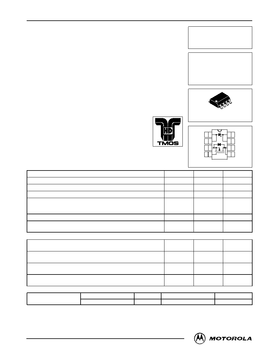
CASE 751–06, Style 18
(SO– 8)
1
2
3
4
8
7
6
5
A
S
G
C
D
TOP VIEW
Motorola, Inc. 1998
相关PDF资料 |
PDF描述 |
|---|---|
| MMDFS6N303R2 | 6 A, 30 V, 0.035 ohm, N-CHANNEL, Si, POWER, MOSFET |
| MMDFS6N303 | 6 A, 30 V, 0.035 ohm, N-CHANNEL, Si, POWER, MOSFET |
| MMFT3055VT3G | 1700 mA, 60 V, N-CHANNEL, Si, SMALL SIGNAL, MOSFET, TO-261AA |
| MMFT3055VT3 | 1700 mA, 60 V, N-CHANNEL, Si, SMALL SIGNAL, MOSFET, TO-261AA |
| MMFT6661T1 | 500 mA, 90 V, N-CHANNEL, Si, SMALL SIGNAL, MOSFET, TO-261AA |
相关代理商/技术参数 |
参数描述 |
|---|---|
| MMDFS6N303R2 | 功能描述:MOSFET N-CH 30V 6A 8-SOIC RoHS:否 类别:分离式半导体产品 >> FET - 单 系列:FETKY™ 标准包装:1,000 系列:MESH OVERLAY™ FET 型:MOSFET N 通道,金属氧化物 FET 特点:逻辑电平门 漏极至源极电压(Vdss):200V 电流 - 连续漏极(Id) @ 25° C:18A 开态Rds(最大)@ Id, Vgs @ 25° C:180 毫欧 @ 9A,10V Id 时的 Vgs(th)(最大):4V @ 250µA 闸电荷(Qg) @ Vgs:72nC @ 10V 输入电容 (Ciss) @ Vds:1560pF @ 25V 功率 - 最大:40W 安装类型:通孔 封装/外壳:TO-220-3 整包 供应商设备封装:TO-220FP 包装:管件 |
| MMDJ3N03BJT | 制造商:ONSEMI 制造商全称:ON Semiconductor 功能描述:Plastic Power Transistors SO−8 for Surface Mount Applications |
| MMDJ3P03BJT | 制造商:MOTOROLA 制造商全称:Motorola, Inc 功能描述:DUAL BIPOLAR POWER TRANSISTOR PNP SILICON 30 VOLTS 3 AMPERES |
| MMDJ-65608EV-30 | 制造商:ATMEL 制造商全称:ATMEL Corporation 功能描述:Rad. Tolerant 128K x 8 Very Low Power 5V CMOS SRAM |
| MMDJ-65608EV-30-E | 制造商:ATMEL 制造商全称:ATMEL Corporation 功能描述:Rad. Tolerant 128K x 8 Very Low Power 5V CMOS SRAM |
发布紧急采购,3分钟左右您将得到回复。