- 您现在的位置:买卖IC网 > PDF目录45336 > MN101CP54CAL (PANASONIC CORP) 8-BIT, OTPROM, 20 MHz, MICROCONTROLLER, PQFP80 PDF资料下载
参数资料
| 型号: | MN101CP54CAL |
| 厂商: | PANASONIC CORP |
| 元件分类: | 微控制器/微处理器 |
| 英文描述: | 8-BIT, OTPROM, 20 MHz, MICROCONTROLLER, PQFP80 |
| 封装: | 14 X 14 MM, 0.65 MM PITCH, PLASTIC, LQFP-80 |
| 文件页数: | 224/544页 |
| 文件大小: | 2900K |
| 代理商: | MN101CP54CAL |
第1页第2页第3页第4页第5页第6页第7页第8页第9页第10页第11页第12页第13页第14页第15页第16页第17页第18页第19页第20页第21页第22页第23页第24页第25页第26页第27页第28页第29页第30页第31页第32页第33页第34页第35页第36页第37页第38页第39页第40页第41页第42页第43页第44页第45页第46页第47页第48页第49页第50页第51页第52页第53页第54页第55页第56页第57页第58页第59页第60页第61页第62页第63页第64页第65页第66页第67页第68页第69页第70页第71页第72页第73页第74页第75页第76页第77页第78页第79页第80页第81页第82页第83页第84页第85页第86页第87页第88页第89页第90页第91页第92页第93页第94页第95页第96页第97页第98页第99页第100页第101页第102页第103页第104页第105页第106页第107页第108页第109页第110页第111页第112页第113页第114页第115页第116页第117页第118页第119页第120页第121页第122页第123页第124页第125页第126页第127页第128页第129页第130页第131页第132页第133页第134页第135页第136页第137页第138页第139页第140页第141页第142页第143页第144页第145页第146页第147页第148页第149页第150页第151页第152页第153页第154页第155页第156页第157页第158页第159页第160页第161页第162页第163页第164页第165页第166页第167页第168页第169页第170页第171页第172页第173页第174页第175页第176页第177页第178页第179页第180页第181页第182页第183页第184页第185页第186页第187页第188页第189页第190页第191页第192页第193页第194页第195页第196页第197页第198页第199页第200页第201页第202页第203页第204页第205页第206页第207页第208页第209页第210页第211页第212页第213页第214页第215页第216页第217页第218页第219页第220页第221页第222页第223页当前第224页第225页第226页第227页第228页第229页第230页第231页第232页第233页第234页第235页第236页第237页第238页第239页第240页第241页第242页第243页第244页第245页第246页第247页第248页第249页第250页第251页第252页第253页第254页第255页第256页第257页第258页第259页第260页第261页第262页第263页第264页第265页第266页第267页第268页第269页第270页第271页第272页第273页第274页第275页第276页第277页第278页第279页第280页第281页第282页第283页第284页第285页第286页第287页第288页第289页第290页第291页第292页第293页第294页第295页第296页第297页第298页第299页第300页第301页第302页第303页第304页第305页第306页第307页第308页第309页第310页第311页第312页第313页第314页第315页第316页第317页第318页第319页第320页第321页第322页第323页第324页第325页第326页第327页第328页第329页第330页第331页第332页第333页第334页第335页第336页第337页第338页第339页第340页第341页第342页第343页第344页第345页第346页第347页第348页第349页第350页第351页第352页第353页第354页第355页第356页第357页第358页第359页第360页第361页第362页第363页第364页第365页第366页第367页第368页第369页第370页第371页第372页第373页第374页第375页第376页第377页第378页第379页第380页第381页第382页第383页第384页第385页第386页第387页第388页第389页第390页第391页第392页第393页第394页第395页第396页第397页第398页第399页第400页第401页第402页第403页第404页第405页第406页第407页第408页第409页第410页第411页第412页第413页第414页第415页第416页第417页第418页第419页第420页第421页第422页第423页第424页第425页第426页第427页第428页第429页第430页第431页第432页第433页第434页第435页第436页第437页第438页第439页第440页第441页第442页第443页第444页第445页第446页第447页第448页第449页第450页第451页第452页第453页第454页第455页第456页第457页第458页第459页第460页第461页第462页第463页第464页第465页第466页第467页第468页第469页第470页第471页第472页第473页第474页第475页第476页第477页第478页第479页第480页第481页第482页第483页第484页第485页第486页第487页第488页第489页第490页第491页第492页第493页第494页第495页第496页第497页第498页第499页第500页第501页第502页第503页第504页第505页第506页第507页第508页第509页第510页第511页第512页第513页第514页第515页第516页第517页第518页第519页第520页第521页第522页第523页第524页第525页第526页第527页第528页第529页第530页第531页第532页第533页第534页第535页第536页第537页第538页第539页第540页第541页第542页第543页第544页
Chapter 1
Overview
I - 14
Pin Description
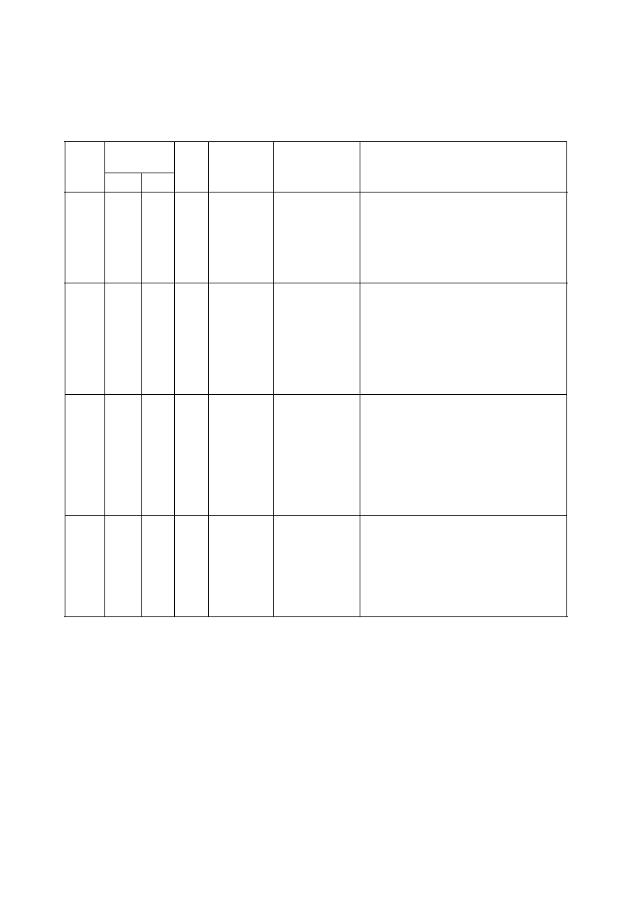
Table 1-3-5
Pin Function Summary (4/7)
Name
No.
I/O
Other
Function
Description
80LQFP
84QFP
SBI0
SBI2
29
32
31
34
Input
P01, RXD
P04
Serial interface
received data input
pins
Receive data output pins for serial interfaces 0 , 2.
Pull-up and pull-down resistors can be selected by the
P0PLUD register. Select input mode by the P0DIR
register, and serial input mode by the serial mode
register 1 ( SC0MD1, SC2MD1).
These can be used as normal I/O pins when the serial
interface is not used.
SBT0
SBT2
30
33
32
35
I/O
P02
P05
Serial interface clock
I/O pins
Clock I/O pins for serial interfaces 0 , 2.
The output configuration, either CMOS push-pull or n-
channel open-drain can be selected. Pull-up and pull-
down resi stors can be selected by the P0PLUD
register. Select clock I/O for each communication mode
by the P0DIR register and serial mode register 1
( SC0MD1, SC2MD1).
These can be used as normal I/O pins when the serial
interface is not used.
TXD
28
30
Output
SBO0, P00
UART transmission
data output pins
In the seri al i nterface i n UART mode, thi s pi n i s
configured as the transmission data output pin.
The output configuration, either CMOS push-pull or n-
channel open-drain can be selected. Pull-up and pull-
down resi stors can be selected by the P0PLUD
resister.
Select output mode by the P0DIR register, and serial
data output by serial 0 mode register 1 ( SC0MD1).
This canbe used as normal I/O pinwhenthe serial
interface is not used.
RXD
29
31
Input
SBI0, P01
UART received data
input pin
In the seri al i nterface i n UART mode, thi s pi n i s
configured as the received data input pin.
Pull-up and pull-down resistors can be selected by the
P0PLUD register. Set this pin to the input mode by the
P0DIR register, and to the serial input mode by the
serial 0 mode register 1 ( SC0MD1).
This canbe used as normal I/O pinwhenthe serial
interface is not used.
相关PDF资料 |
PDF描述 |
|---|---|
| MN101CF73A | 8-BIT, FLASH, 10 MHz, MICROCONTROLLER, PQFP64 |
| MN101D01Y | 8-BIT, OTPROM, MICROCONTROLLER, PQFP100 |
| MN101D01F | 8-BIT, OTPROM, MICROCONTROLLER, PQFP100 |
| MN102H60M | 16-BIT, MROM, 34 MHz, MICROCONTROLLER, PQFP100 |
| MN103SB5K | 32-BIT, MROM, 60 MHz, MICROCONTROLLER, PQFP64 |
相关代理商/技术参数 |
参数描述 |
|---|---|
| MN101CP66D | 制造商:PANASONIC 制造商全称:Panasonic Semiconductor 功能描述:MN101C66D |
| MN101D01FPA4 | 制造商:Panasonic Industrial Company 功能描述:IC |
| MN101D01GPC1 | 制造商:Panasonic Industrial Company 功能描述:IC |
| MN101D02D | 制造商:PANASONIC 制造商全称:Panasonic Semiconductor 功能描述:Microcomputers/Controllers |
| MN101D02F | 制造商:PANASONIC 制造商全称:Panasonic Semiconductor 功能描述:Microcomputers/Controllers |
发布紧急采购,3分钟左右您将得到回复。