- 您现在的位置:买卖IC网 > PDF目录45359 > MPC8306VMABDCA (FREESCALE SEMICONDUCTOR INC) 32-BIT, 133 MHz, RISC PROCESSOR, PBGA369 PDF资料下载
参数资料
| 型号: | MPC8306VMABDCA |
| 厂商: | FREESCALE SEMICONDUCTOR INC |
| 元件分类: | 微控制器/微处理器 |
| 英文描述: | 32-BIT, 133 MHz, RISC PROCESSOR, PBGA369 |
| 封装: | 19 X 19 MM, 1.61 MM HEIGHT, 0.80 MM PITCH, LEAD FREE, MAPBGA-369 |
| 文件页数: | 5/76页 |
| 文件大小: | 474K |
| 代理商: | MPC8306VMABDCA |
第1页第2页第3页第4页当前第5页第6页第7页第8页第9页第10页第11页第12页第13页第14页第15页第16页第17页第18页第19页第20页第21页第22页第23页第24页第25页第26页第27页第28页第29页第30页第31页第32页第33页第34页第35页第36页第37页第38页第39页第40页第41页第42页第43页第44页第45页第46页第47页第48页第49页第50页第51页第52页第53页第54页第55页第56页第57页第58页第59页第60页第61页第62页第63页第64页第65页第66页第67页第68页第69页第70页第71页第72页第73页第74页第75页第76页
MPC8306 PowerQUICC II Pro Integrated Communications Processor Family Hardware Specifications, Rev. 0
Freescale Semiconductor
13
RESET Initialization
5
RESET Initialization
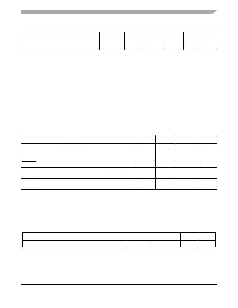
This section describes the AC electrical specifications for the reset initialization timing requirements of
the MPC8306. Table 9 provides the reset initialization AC timing specifications for the reset
component(s).
Table 10 provides the PLL lock times.
5.1
Reset Signals DC Electrical Characteristics
Table 11 provides the DC electrical characteristics for the MPC8306 reset signals mentioned in Table 9.
SYS_CLK_IN duty cycle
tKHK/tSYS_CLK_
IN
40
—
60
%
3
SYS_CLK_IN jitter
—
±150
ps
4, 5
Notes:
1. Caution: The system, core and QUICC Engine block must not exceed their respective maximum or minimum operating
frequencies.
2. Rise and fall times for SYS_CLK_IN are measured at 0.33 and 2.97 V.
3. Timing is guaranteed by design and characterization.
4. This represents the total input jitter—short term and long term—and is guaranteed by design.
5. The SYS_CLK_IN driver’s closed loop jitter bandwidth should be < 500 kHz at –20 dB. The bandwidth must be set low to
allow cascade-connected PLL-based devices to track SYS_CLK_IN drivers with the specified jitter.
6. Spread spectrum is allowed upto 1% down-spread @ 33kHz (max rate).
Table 9. RESET Initialization Timing Specifications
Parameter/Condition
Min
Max
Unit
Notes
Required assertion time of HRESET to activate reset flow
32
—
tSYS_CLK_IN
1
Required assertion time of PORESET with stable clock applied to
SYS_CLK_IN
32
—
tSYS_CLK_IN
1
HRESET assertion (output)
512
—
tSYS_CLK_IN
1
Input setup time for POR configuration signals
(CFG_RESET_SOURCE[0:3]) with respect to negation of PORESET
4—
tSYS_CLK_IN
1, 2
Input hold time for POR config signals with respect to negation of
HRESET
0
—
ns
1, 2
Notes:
1. tSYS_CLK_IN is the clock period of the input clock applied to SYS_CLK_IN. For more details, see the MPC8306
PowerQUICC II Pro Integrated Communications Processor Reference Manual
.
2. POR configuration signals consists of CFG_RESET_SOURCE[0:3].
Table 10. PLL Lock Times
Parameter/Condition
Min
Max
Unit
Notes
PLL lock times
—
100
s—
Table 8. SYS_CLK_IN AC Timing Specifications
相关PDF资料 |
PDF描述 |
|---|---|
| MPC8306CVMADDCA | 32-BIT, 266 MHz, RISC PROCESSOR, PBGA369 |
| MPC8308CZQAGD | 32-BIT, 266 MHz, MICROPROCESSOR, PBGA473 |
| MPC8308CZQADD | 32-BIT, 266 MHz, MICROPROCESSOR, PBGA473 |
| MPC8308CVMAFD | 32-BIT, 266 MHz, MICROPROCESSOR, PBGA473 |
| MPC8309CVMAGDCA | 32-BIT, 400 MHz, RISC PROCESSOR, PBGA489 |
相关代理商/技术参数 |
参数描述 |
|---|---|
| MPC8306VMACDC | 制造商:Freescale Semiconductor 功能描述:MPC8306VMACDC - Bulk |
| MPC8306VMACDCA | 功能描述:微处理器 - MPU E300 MP 200 RoHS:否 制造商:Atmel 处理器系列:SAMA5D31 核心:ARM Cortex A5 数据总线宽度:32 bit 最大时钟频率:536 MHz 程序存储器大小:32 KB 数据 RAM 大小:128 KB 接口类型:CAN, Ethernet, LIN, SPI,TWI, UART, USB 工作电源电压:1.8 V to 3.3 V 最大工作温度:+ 85 C 安装风格:SMD/SMT 封装 / 箱体:FBGA-324 |
| MPC8306VMADDC | 制造商:Freescale Semiconductor 功能描述:MPC8306VMADDC - Bulk |
| MPC8306VMADDCA | 功能描述:微处理器 - MPU E300 MP 266 RoHS:否 制造商:Atmel 处理器系列:SAMA5D31 核心:ARM Cortex A5 数据总线宽度:32 bit 最大时钟频率:536 MHz 程序存储器大小:32 KB 数据 RAM 大小:128 KB 接口类型:CAN, Ethernet, LIN, SPI,TWI, UART, USB 工作电源电压:1.8 V to 3.3 V 最大工作温度:+ 85 C 安装风格:SMD/SMT 封装 / 箱体:FBGA-324 |
| MPC8306VMADDCA | 制造商:Freescale Semiconductor 功能描述:IC 32-BIT MPU 266 MHz 369-LFBGA |
发布紧急采购,3分钟左右您将得到回复。