- 您现在的位置:买卖IC网 > PDF目录3948 > MPC8313ZQADD (Freescale Semiconductor)IC MPU POWERQUICC II PRO 516PBGA PDF资料下载
参数资料
| 型号: | MPC8313ZQADD |
| 厂商: | Freescale Semiconductor |
| 文件页数: | 6/99页 |
| 文件大小: | 0K |
| 描述: | IC MPU POWERQUICC II PRO 516PBGA |
| 标准包装: | 40 |
| 系列: | MPC83xx |
| 处理器类型: | 32-位 MPC83xx PowerQUICC II Pro |
| 速度: | 267MHz |
| 电压: | 0.95 V ~ 1.05 V |
| 安装类型: | 表面贴装 |
| 封装/外壳: | 516-BBGA 裸露焊盘 |
| 供应商设备封装: | 516-PBGAPGE(27x27) |
| 包装: | 托盘 |
| 配用: | MPC8313E-RDB-ND - BOARD PROCESSOR |
第1页第2页第3页第4页第5页当前第6页第7页第8页第9页第10页第11页第12页第13页第14页第15页第16页第17页第18页第19页第20页第21页第22页第23页第24页第25页第26页第27页第28页第29页第30页第31页第32页第33页第34页第35页第36页第37页第38页第39页第40页第41页第42页第43页第44页第45页第46页第47页第48页第49页第50页第51页第52页第53页第54页第55页第56页第57页第58页第59页第60页第61页第62页第63页第64页第65页第66页第67页第68页第69页第70页第71页第72页第73页第74页第75页第76页第77页第78页第79页第80页第81页第82页第83页第84页第85页第86页第87页第88页第89页第90页第91页第92页第93页第94页第95页第96页第97页第98页第99页
MPC8313E PowerQUICC II Pro Processor Hardware Specifications, Rev. 4
14
Freescale Semiconductor
5.2
RESET AC Electrical Characteristics
This table provides the reset initialization AC timing specifications.
This table provides the PLL lock times.
6
DDR and DDR2 SDRAM
This section describes the DC and AC electrical specifications for the DDR SDRAM interface. Note that
DDR SDRAM is GVDD(typ) = 2.5 V and DDR2 SDRAM is GVDD(typ) = 1.8 V.
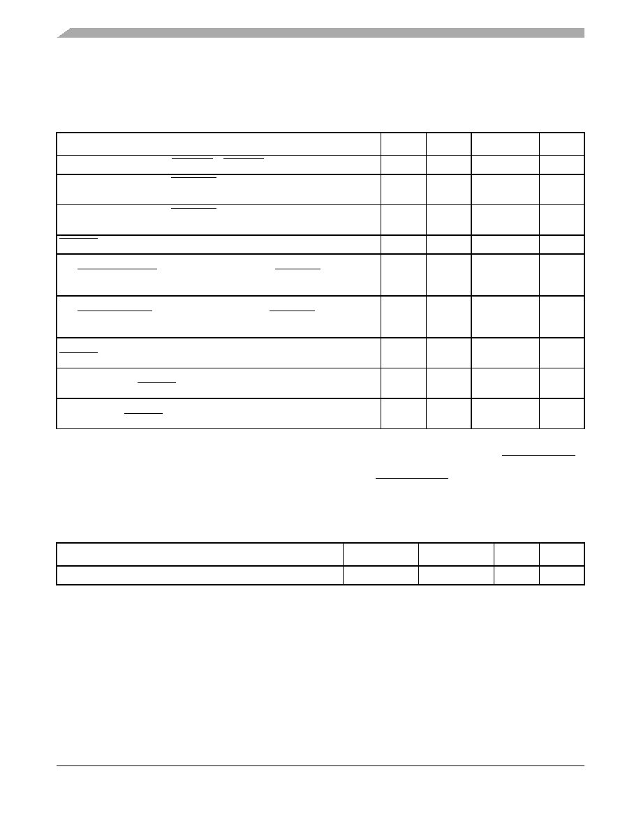
Table 10. RESET Initialization Timing Specifications
Parameter/Condition
Min
Max
Unit
Note
Required assertion time of HRESET or SRESET (input) to activate reset flow
32
—
tPCI_SYNC_IN
1
Required assertion time of PORESET with stable clock and power applied to
SYS_CLK_IN when the device is in PCI host mode
32
—
tSYS_CLK_IN
2
Required assertion time of PORESET with stable clock and power applied to
PCI_SYNC_IN when the device is in PCI agent mode
32
—
tPCI_SYNC_IN
1
HRESET assertion (output)
512
—
tPCI_SYNC_IN
1
Input setup time for POR configuration signals (CFG_RESET_SOURCE[0:3]
and CFG_CLK_IN_DIV) with respect to negation of PORESET when the
device is in PCI host mode
4—
tSYS_CLK_IN
2
Input setup time for POR configuration signals (CFG_RESET_SOURCE[0:2]
and CFG_CLKIN_DIV) with respect to negation of PORESET when the
device is in PCI agent mode
4—
tPCI_SYNC_IN
1
Input hold time for POR configuration signals with respect to negation of
HRESET
0—
ns
—
Time for the device to turn off POR configuration signal drivers with respect
to the assertion of HRESET
—4
ns
3
Time for the device to turn on POR configuration signal drivers with respect to
the negation of HRESET
1—
tPCI_SYNC_IN
1, 3
Notes:
1. tPCI_SYNC_IN is the clock period of the input clock applied to PCI_SYNC_IN. When the device is In PCI host mode the
primary clock is applied to the SYS_CLK_IN input, and PCI_SYNC_IN period depends on the value of CFG_CLKIN_DIV.
2. tSYS_CLK_IN is the clock period of the input clock applied to SYS_CLK_IN. It is only valid when the device is in PCI host mode.
3. POR configuration signals consists of CFG_RESET_SOURCE[0:2] and CFG_CLKIN_DIV.
Table 11. PLL Lock Times
Parameter/Condition
Min
Max
Unit
Note
PLL lock times
—
100
s—
相关PDF资料 |
PDF描述 |
|---|---|
| 3-1734592-1 | CONN FPC 31POS .5MM RT ANG SMD |
| 346-012-526-804 | CARDEDGE 12POS DUAL .125 GREEN |
| 346-012-526-802 | CARDEDGE 12POS DUAL .125 GREEN |
| MPC8313VRAFF | IC MPU POWERQUICC II PRO 516PBGA |
| MPC8313EZQAFF | IC MPU POWERQUICC II PRO 516PBGA |
相关代理商/技术参数 |
参数描述 |
|---|---|
| MPC8313ZQADDB | 功能描述:微处理器 - MPU REV2.1 W/OENCR RoHS:否 制造商:Atmel 处理器系列:SAMA5D31 核心:ARM Cortex A5 数据总线宽度:32 bit 最大时钟频率:536 MHz 程序存储器大小:32 KB 数据 RAM 大小:128 KB 接口类型:CAN, Ethernet, LIN, SPI,TWI, UART, USB 工作电源电压:1.8 V to 3.3 V 最大工作温度:+ 85 C 安装风格:SMD/SMT 封装 / 箱体:FBGA-324 |
| MPC8313ZQADDC | 功能描述:微处理器 - MPU 8313 REV2.2 PB NO ENC RoHS:否 制造商:Atmel 处理器系列:SAMA5D31 核心:ARM Cortex A5 数据总线宽度:32 bit 最大时钟频率:536 MHz 程序存储器大小:32 KB 数据 RAM 大小:128 KB 接口类型:CAN, Ethernet, LIN, SPI,TWI, UART, USB 工作电源电压:1.8 V to 3.3 V 最大工作温度:+ 85 C 安装风格:SMD/SMT 封装 / 箱体:FBGA-324 |
| MPC8313ZQAFD | 制造商:FREESCALE 制造商全称:Freescale Semiconductor, Inc 功能描述:PowerQUICC? II Pro Processor Hardware Specifications |
| MPC8313ZQAFDA | 制造商:FREESCALE 制造商全称:Freescale Semiconductor, Inc 功能描述:PowerQUICC? II Pro Processor Hardware Specifications |
| MPC8313ZQAFDB | 制造商:FREESCALE 制造商全称:Freescale Semiconductor, Inc 功能描述:PowerQUICC? II Pro Processor Hardware Specifications |
发布紧急采购,3分钟左右您将得到回复。